I would try another i2s source without i2s attenuation and you might try textbook DEM clocking. Just for checking reasons. Cheers
HI...
I immediately admit that I don't have the technical skills to be able to follow the discussions of the group....
I need to manage an i2s stream (lrck + bck + data) coming from multiple sources (cd transport/usb card) through rj45 connector.
I would like to push my one
tda1541 (I already know I should use simultaneous mode) at least up to 192khz 24bit.
Could someone then tell me how to get my target correctly?
Thanks in advance to anyone who wants to help me.
Antonio
Hi,
The asking is not clear. Can you explain the need more in detail. From what you say I understand you want to connect multiple sources on a card that is outputting I2S through RJ45 outputting I2S towards the tda 1541A dac.
The asking is not clear. Can you explain the need more in detail. From what you say I understand you want to connect multiple sources on a card that is outputting I2S through RJ45 outputting I2S towards the tda 1541A dac.
Yes, you understood correctly .. obviously I have only one RJ45 socket and I alternate the two sources via LAN cable.
As far as USB is concerned, the data flow is Raspberry to jlsound (first version) then i2s via RJ45 connectivity at the input of my DAC.
Obviously using Qobuz I also need to play 192/24bit files which I currently cannot play.
As far as USB is concerned, the data flow is Raspberry to jlsound (first version) then i2s via RJ45 connectivity at the input of my DAC.
Obviously using Qobuz I also need to play 192/24bit files which I currently cannot play.
you mean you are not using tcp/ip but simply use a rj45 cable as a wire transporting via three pairs the I2S protocol and the return GND inside each of the pair ?
Maybe you should use just good golded relays with a switch pot to swap from each. Impedance of those cables and RJ45 are not the same than the traces of most pcb designs, so the shorter would be the better in your design. Alas relays and length will certainly not the best for the loss.
a balanced design could perhaps be sligthy better to route I2S signal.
So a switching board with relays just before the sim mode board is the best bet. Unfornatully not sure it is the best way for quality. the quality of the front end is important for the sound, not only the dac chip. So all those length of cables between the boards are really not advised !
I would just continue to switch by hand when needed and find a sim board in witch I wire at the input the RJ45 connector inside the dac box, in order the sim board to be the closest of the dac chip board. Remember the 1541A dac chip needs different power supply pins when seing sim mode and not I2S mode.
at the outside of the dac box the RJ45 wire should be as short as possible as the sources (JLSOUNDS and CD transport) are clocking the DAC.
If designing a switching board with relay it certainly asks to open a specific thread to have a better help.
Yes, I already know the balanced i2s transport technique, I'm already using it via amls31/32 transmitter/receiver.
I didn't mention to simplify.
I also know how to switch i2s with logic gates.
But that's not the point here.
Here we talk about how to get at least 192khz/24bit from tda1541

I didn't mention to simplify.
I also know how to switch i2s with logic gates.
But that's not the point here.
Here we talk about how to get at least 192khz/24bit from tda1541

IMHO, that design is suffering of a high jitter and is not made for high quality playback whatever it is 16/41 or 24/192, simultaneous mode or not.
Best bet is to put a fifo buffer and reclocking just before the sim board where here the cable length will be short within less than 10 cm between the reclocking and the dac chip. Maybe IanCanada 2 blocks classic fifo board and reclcok board : despite being two boards they share some logic and must work together (they were sold in two boards more for commercial reasons i believe). This design is imputing I2S and outputing clean reclocked I2s.
Then you can put any passive sim board or a fgpa based one as the Iant I2S to PCM board that can be slavered by this clock for jitter reason and can outputt sim mode for tda1541A and few pcm other chips (ad1862, pcm63, pcm1704, pcm56, etc). I have 4 of those board if interested by one if you need one.
Despite you use balanced with the cables I really use in your shoes a dedicated gnd return cable by pair, so each shielded and isolated from the gnd return cable of the other pairs. Should be feasible with the lastest high speed tcp/ip cables which pairs are all shielded.
I cam report that I was using digital balanced transmission with theese pairs AM26LS31 / AM26LS32.
Even in "no-need-for" short connections.
And sound always was significantly better. I cant explain why?
Althouht this termination of 50ohm might be so low, inspired the datasheet recomm... I think that i used larger value 220ohms to 1K.
And with a resistors in each line for the signal inefrity. to eliminate spikess at the edges and reduce ground bounces... Google for signal integrity.
Cant remember now 🙁 BUT that could be maesured with a scope and chope what is better? I did that way...
.
With enable function at every chip You can acheive a selection in addition when nedded. BUT and transmitter and receiver should be EN or DISS in the same time...
.
Another feature is that You can have inverted DATA line, by simple routing transmitter +out to recever -in and tr -out to rec +in
.
Off course that other trans/rec pairs could be used. The principle remains the same.
.
Note!
With this pair current consumption is not small and it is significantly larger frim common digital ICs. Before making final PS try to measure and consult datasheet about current consumption. Also the chips are getting little bit hot, but not so much so it can be used without heatsink.
.
Last edited:
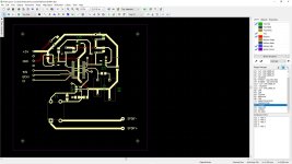
Hello everyone ,
I finally finish to read the all thread , and comes to the idea to build the DAC as per John from Ecdesigns
the TDA1541A Dual Mono 17 bit Signed Magnitude DAC
I want to do it as close to his recommendations as possible , here are the first attempts to get pcb from his notes and shematics :
I/V out will be passive , a pairs of Sowters 1465
any thought are welcome 😉
Attachments
Last edited:
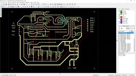
If you real want to male it ultimate, make it four Layer with solids ground and power planes.
Four layers is out of my reach and I am not sure it is worth it , may John have some thoughts on that
but there will be some copper pour on most of the pcb's for the gnd plane
.
but there will be some copper pour on most of the pcb's for the gnd plane
.
Copper pour will be on the bottom side , where most of the ground connexions are , if by shape you meam the width of the trace , I will grown them as much as possible , it is difficult to be large enought and far from other trace
I am a beginner and have a lot to learn 🙂
.
I am a beginner and have a lot to learn 🙂
.
Dedicate a bit more time and willingness to learn, and design it 4 layer 🙂 It's very affordable now, and why not use that chance 🙂
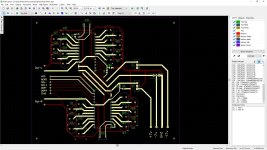
Here's another recent take on the "ultimate TDA1541":
https://www.mvaudiolabs.com/digital/tda1541a-reference-dac/
nice solution for the I2S/simultaneous attenuation and much more.
And regarding the layout: try to keep traces on one layer only, make the traces on the other layer as short as possible, returning them as soon as possible to the designated "signal layer". The other layer shall be your "ground layer".
For PCBs with THT, that basically means top layer = ground layer, while bottom layer = signal layer. Use multiple vias when changing layers (reduces via inductance).
Last edited:
Интересная статья, спасибо.
 Please post in English.
Especially dem capacitors leakage and return of unselected bitcurrents to +5v.Интересная статья, спасибо.
- Home
- Source & Line
- Digital Line Level
- Building the ultimate NOS DAC using TDA1541A