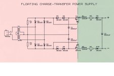
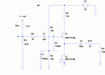
Hi,
See attached picture of FCTS
Regards,
Marcel
Hi, Marcel,
The main problem I see with this particular charge-transfer topology is that it still doesn't effectively isolate the powered circuit from A.C. line noise. While C1 is disconnected from the A.C. line by the periodic commutation of D5 and D6, any A.C. line noise still modulates the base of T1. Which means the current supplied to the powered circuit from C1 will be a modulated replica of that noise. The same noise breakthrough mechanism will happen with C2, T2, D7, and D8 during the opposite half-cycle.
Hi Ken,
It's not my design,I just digged this up as was asked for this schema.
It's one of EcDesigns old approaches.
Marcel
It's not my design,I just digged this up as was asked for this schema.
It's one of EcDesigns old approaches.
Marcel
Hi, -ecdesigns-The rise time inside the TDA1541A is determined by its specified limiting frequency of 6.4 MHz. This corresponds with a signal rise time of approx. 56ns.
How you this has estimated?
According to Philips datasheet (TDA1541A, p.7), rise time (fall time) <32 ns.
On the TDA1541A inputs stand the transistors but diodes connected with output of TDA1541A.Each TDA1541A I2S input has a diode in series that stops conducting when the external signal amplitude exceeds approx. 1.4V. In other words, the external drive circuit is disconnected when the input diode stops conducting.
See: ″A Monolithic Dual 16-Bit D/A Converter″, ieee journal of solid-state circuits, vol. sc-21, no. 3, june 1986 and see attachment.

The value of the resistor must be close to wave resistance of the signal line to prevent the signal reflections. For PCB conductors this resistance has an order 100 ohm (nowhere near not 1k and not 1,8k). 1,8k - in any event too muchBased on this, the limiting series resistor value for TDA1541A BCK, WS, and DATA inputs would be 1K8
It is impossible with impunity enlarge duration a rise time of input signal. This enlarges the uncertainty of the switching, but signifies and jitters.
Serg
Attachments
Hi SSerg,
I used this online calculator:
Pronine Electronics Design - RC Circuit Calculator
Using 6.4 MHz and 12pF (input capacitance). Differences between datasheet and calculation can be explained by the CCS in the I2S input circuit
TDA1541A I2S input circuit is similar to the TDA1543 (attached schematic diagram).
Correct, and in the past I used series resistor values ranging from 22 Ohms to around 150 Ohms. In the Octal DI DAC project I used 22 OHms if I am correct.
The reason I use (much) higher series resistor values is to avoid injecting more RF energy than neccessary for reliable chip operation. I use I2S attenuators with 800mVpp output signal amplitude for similar reason.
TDA1541A still works correctly with series resistors up to 1K Ohm (up to 96 KHz sample rate in NOS). When using 44.1 KHz exclusively TDA1541A still works correctly with series resistors up to 1K8.
I use an extra safety margin by using 560R series resistor for BCK, this will enable sample rates up to 96 KHz NOS (64 bits / frame) or 192 KHz NOS (32 bits / frame).
Until recently I was convinced that fastest transients would lead to lower trigger uncertainty and thus lower jitter. However, faster transients can result in increased ground-bounce that in turn can lead to even higher trigger uncertainty. So an optimum must be found between transient rise / fall time and generated jitter.
When using fast logic of say 275MHz that drives a slow TDA1541A (6.4 MHz) we run into compatibility issues that can result in high jitter levels. That's why we need I2S signal band limiting and I2S signal attenuation. WS and DATA signals are not used for sample timing and only need to be stable when latched by the BCK signal rising transient, so here fast transients only increase the amount of interference being dumped on the chip substrate as a result of signal transients. This WS and DATA induced ground-bounce can in turn lead to increased on-chip BCK jitter.
How you this has estimated?
According to Philips datasheet (TDA1541A, p.7), rise time (fall time) <32 ns.
I used this online calculator:
Pronine Electronics Design - RC Circuit Calculator
Using 6.4 MHz and 12pF (input capacitance). Differences between datasheet and calculation can be explained by the CCS in the I2S input circuit
On the TDA1541A inputs stand the transistors but diodes connected with output of TDA1541A.
See: ″A Monolithic Dual 16-Bit D/A Converter″, ieee journal of solid-state circuits, vol. sc-21, no. 3, june 1986 and see attachment.
TDA1541A I2S input circuit is similar to the TDA1543 (attached schematic diagram).
The value of the resistor must be close to wave resistance of the signal line to prevent the signal reflections. For PCB conductors this resistance has an order 100 ohm (nowhere near not 1k and not 1,8k). 1,8k - in any event too much
Correct, and in the past I used series resistor values ranging from 22 Ohms to around 150 Ohms. In the Octal DI DAC project I used 22 OHms if I am correct.
The reason I use (much) higher series resistor values is to avoid injecting more RF energy than neccessary for reliable chip operation. I use I2S attenuators with 800mVpp output signal amplitude for similar reason.
TDA1541A still works correctly with series resistors up to 1K Ohm (up to 96 KHz sample rate in NOS). When using 44.1 KHz exclusively TDA1541A still works correctly with series resistors up to 1K8.
I use an extra safety margin by using 560R series resistor for BCK, this will enable sample rates up to 96 KHz NOS (64 bits / frame) or 192 KHz NOS (32 bits / frame).
It is impossible with impunity enlarge duration a rise time of input signal. This enlarges the uncertainty of the switching, but signifies and jitters.
Until recently I was convinced that fastest transients would lead to lower trigger uncertainty and thus lower jitter. However, faster transients can result in increased ground-bounce that in turn can lead to even higher trigger uncertainty. So an optimum must be found between transient rise / fall time and generated jitter.
When using fast logic of say 275MHz that drives a slow TDA1541A (6.4 MHz) we run into compatibility issues that can result in high jitter levels. That's why we need I2S signal band limiting and I2S signal attenuation. WS and DATA signals are not used for sample timing and only need to be stable when latched by the BCK signal rising transient, so here fast transients only increase the amount of interference being dumped on the chip substrate as a result of signal transients. This WS and DATA induced ground-bounce can in turn lead to increased on-chip BCK jitter.
Attachments

Using 6.4 MHz and 12pF (input capacitance).
You try to define rise time under two parameters. This is incorrect. Rise time (slew rate) is defined as minimum three parameters: frequency of the signal, amplitude of the signal and capacity of the load. For sine it is enough three specified parameter. Additional parameters are required for signal with other form, characterizing the signal form. In any event, it is necessary be orientated on producer data.
TDA1541A I2S input circuit is similar to the TDA1543 (attached schematic diagram).
I do not know, as beside TDA1543. But on TDA1541A I have studied much material and can confirm that you mistaken.
Here is circuit (see attachment) from monograph "High-speed and high-resolution analog-to-digital and digital-to-analog converters", R.J van de Plassche, 1989. This work is dedicated to family TDA1540, TDA1541(A). Obviously that diode unites with output, but at the input stands the transistor.
When using 44.1 KHz exclusively TDA1541A still works correctly with series resistors up to 1K8.
As be with reflected signals? Furthermore, signal fronts have too low slew rate. This enlarges jitter.
So an optimum must be found between transient rise / fall time and generated jitter.
Think, you bore in mind that needs the reasonable compromise between rise (fall) time and increased ground-bounce. With this it is difficult not to agree.
WS and DATA signals are not used for sample timing and only need to be stable when latched by the BCK signal rising transient
Do not forget that WS defines the moment of the issue of the output signal. The flutter of this moment of time will bring about front flutter of analog signal. Well it?
Attachments
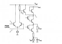
Qustion and suggested buffer/levelshift
Hi All
I have been following this thread for some time now. Facinating!
I am currently using a prototype DAC with much of the technique -ecdesign- uses and it is really showing promise (still a prototype with too long wires, bad screening aso.) .
I have a question regarding the DC shift in I/V stage.
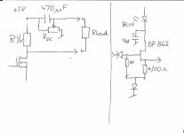
Is this capacitor not as much in the signal path as a coupling capacitor?
See the attached schematic.
Depending on the load resistor, it is not even a correct DC coupling , is it?
And if you use a 470 uF coupling cap. and a load of say 100k , isn¨t this as good as a DC coupling (besides the fact that there is a capacitor in the signal path, witch has its problems)
The other thing is a suggestion to a buffer / level shifter to act on the I2S signals.
Again look at the schematic.
The blue led reduces the 5V to 1,8V witch according to John, should be fin for BCK. A green or red could be used on the WS and DATA signals.
The diode below the source resistor raises the signal to about 0,5V. Maybe this is too muc, but a germanium diode could be used.
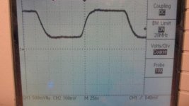
It is a very clean BCK that comes out of this - look at the pictures. Even from the very rude circuit as seen in the last photo.
Comments?
Koldby
Hi All
I have been following this thread for some time now. Facinating!
I am currently using a prototype DAC with much of the technique -ecdesign- uses and it is really showing promise (still a prototype with too long wires, bad screening aso.) .
I have a question regarding the DC shift in I/V stage.
Is this capacitor not as much in the signal path as a coupling capacitor?
See the attached schematic.
Depending on the load resistor, it is not even a correct DC coupling , is it?
And if you use a 470 uF coupling cap. and a load of say 100k , isn¨t this as good as a DC coupling (besides the fact that there is a capacitor in the signal path, witch has its problems)
The other thing is a suggestion to a buffer / level shifter to act on the I2S signals.
Again look at the schematic.
The blue led reduces the 5V to 1,8V witch according to John, should be fin for BCK. A green or red could be used on the WS and DATA signals.
The diode below the source resistor raises the signal to about 0,5V. Maybe this is too muc, but a germanium diode could be used.
It is a very clean BCK that comes out of this - look at the pictures. Even from the very rude circuit as seen in the last photo.
Comments?
Koldby
Attachments
Last edited:
Hello -ecdesigns-
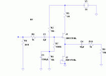
I just found a Pass Lab B1 buffer amp ready made board.
If I do a modification (R4) like in my schematic, can I use it as a IV amp for my TDA1541A ?
Do I need more modifications and which ones ?
Thank you
Bye
Gaetan
I just found a Pass Lab B1 buffer amp ready made board.
If I do a modification (R4) like in my schematic, can I use it as a IV amp for my TDA1541A ?
Do I need more modifications and which ones ?
Thank you
Bye
Gaetan
Attachments
Last edited:
Hi to all,
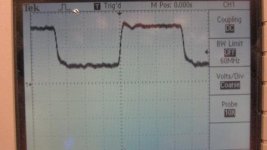
I has decided to look that will if give on DI-DAC square-wave pulse. From diagram is seen that front of the pulse becomes less steep, slew rate falls. The pulse “spreads”.
I has decided to look that will if give on DI-DAC square-wave pulse. From diagram is seen that front of the pulse becomes less steep, slew rate falls. The pulse “spreads”.
Attachments
Last edited:
hello,
apologies for the abrupt enterance. i have retrofitted mr. john b's 2sk170 output (from mark3) on this dac. HiEnd TDA1541 A DAC CS8412 SAA7220 OS Assembled Borad | eBay
i rerouted some traces and cut the others trying my best to disable the discrete circuit, and the sound for the most part a big improvement 😉. (thank you john!) but i'm getting random hf hiss. it's not constant but more of a irregular pulse. any idea what might be causing this?
also i have implemented grundig 9009 dem clock mod which i feel is a must have. what other significant upgrade am i missing out besides the regulators?
i'm eventually wanting to breadboard my own 1541dac following ecdesigns' guidelines and wanting to know what i should put on the must do list.
Last edited:
There is a thread somewhere in which ThorstenL gives his guidelines for doing a breadboard TDA1541a dac which beats most of the commercial tda1541a dacs out there. He incorporates some of his own ideas as well as some of John's.
Look for it using the search function, it's called something like 'best tda1541a implementation' and was running in 2011 I believe...
Look for it using the search function, it's called something like 'best tda1541a implementation' and was running in 2011 I believe...
Hi koldby,
It is in the signal path like elco's in the power supply, but the cap is bypassed by a relatively low resistor value. This improves performance compared to only a cap in the signal path.
The 3 resistor I2S attenuator has proven its effectivity. For BCK I added a RF Schottky diode to split-up the transients in zones with different speed. This enables both, extreme low jitter levels (low ground-bounce) and fast transient within the trigger zone.
Digital scopes have limited resolution (A/D converter), so signals are "forced" to fit in the few pixels on the LCD. This prevents accurate analysis of wave form shape. If you want to observe signals in more detail you will need a suitable large bandwidth analogue scope.
If you -have- to use passive I/V conversion with the I/V resistor tied to GND you have to add a super clean +2mA bias current. This is necessary to create equal signal swing around GND and thus maximise output signal swing with given -25mV and +25mV output compliance.
CCS usually cause problems with perceived sound quality in these applications. If you -have- to use a CCS, then I suggest to use the Aikido circuit where issues with non-linear properties of active elements are largely canceled out. The Aikido circuit can also be translated to JFETs, but I personally prefer the tube version.
Is this capacitor not as much in the signal path as a coupling capacitor?
It is in the signal path like elco's in the power supply, but the cap is bypassed by a relatively low resistor value. This improves performance compared to only a cap in the signal path.
The other thing is a suggestion to a buffer / level shifter to act on the I2S signals.
The 3 resistor I2S attenuator has proven its effectivity. For BCK I added a RF Schottky diode to split-up the transients in zones with different speed. This enables both, extreme low jitter levels (low ground-bounce) and fast transient within the trigger zone.
It is a very clean BCK that comes out of this - look at the pictures. Even from the very rude circuit as seen in the last photo.
Digital scopes have limited resolution (A/D converter), so signals are "forced" to fit in the few pixels on the LCD. This prevents accurate analysis of wave form shape. If you want to observe signals in more detail you will need a suitable large bandwidth analogue scope.
I just found a Pass Lab B1 buffer amp ready made board.
If you -have- to use passive I/V conversion with the I/V resistor tied to GND you have to add a super clean +2mA bias current. This is necessary to create equal signal swing around GND and thus maximise output signal swing with given -25mV and +25mV output compliance.
CCS usually cause problems with perceived sound quality in these applications. If you -have- to use a CCS, then I suggest to use the Aikido circuit where issues with non-linear properties of active elements are largely canceled out. The Aikido circuit can also be translated to JFETs, but I personally prefer the tube version.
Hi PreSapian,
Just like a house requires a solid base, a DAC requires ultra low jitter timing source and ultra clean supply voltages as solid base to build on.
Tweaking a DAC driven by jittery timing signals and noisy supplies is like attempting to build a house on quick sand without solid base and this is likely to end in disaster.
So before even thinking of tweaking the I/V stage it would be wise to make sure you are building on a solid base (ultra low jitter timing signals and ultra clean supply voltages). This will save you years of tweaking that basically lead nowhere. I am speaking out of own experience as I have spent over 6 years tweaking DACs.
Please note that this DAC has massive amounts of jitter. So it is basically impossible to tell if a mod would really improve things without using an ultra low jitter source and ulta clean power supplies as base. Subjective "improvements" could well be a result of added distortion or changed distortion spectrum.
There are many but reducing jitter to lowest possible levels and getting rid of the SAA7220 would be a good start.
apologies for the abrupt enterance. i have retrofitted mr. john b's 2sk170 output (from mark3) on this dac. HiEnd TDA1541 A DAC CS8412 SAA7220 OS Assembled Borad | eBay
Just like a house requires a solid base, a DAC requires ultra low jitter timing source and ultra clean supply voltages as solid base to build on.
Tweaking a DAC driven by jittery timing signals and noisy supplies is like attempting to build a house on quick sand without solid base and this is likely to end in disaster.
So before even thinking of tweaking the I/V stage it would be wise to make sure you are building on a solid base (ultra low jitter timing signals and ultra clean supply voltages). This will save you years of tweaking that basically lead nowhere. I am speaking out of own experience as I have spent over 6 years tweaking DACs.
also i have implemented grundig 9009 dem clock mod which i feel is a must have.
Please note that this DAC has massive amounts of jitter. So it is basically impossible to tell if a mod would really improve things without using an ultra low jitter source and ulta clean power supplies as base. Subjective "improvements" could well be a result of added distortion or changed distortion spectrum.
what other significant upgrade am i missing out besides the regulators?
There are many but reducing jitter to lowest possible levels and getting rid of the SAA7220 would be a good start.
Hi SSerg,
http://www.diyaudio.com/forums/digital-line-level/31780-tda1541-info-3.html
Post #29 and following posts of HtP.
TDA1541A datasheet page 4:
"Input data selection (see also Table 1)
With the input OB/TWC connected to ground, data input (offset binary format) must be in time multiplexed mode. It is accompanied with a word select (WS) and a bit clock input (BCK) signal. The converted samples appear at the output, at the first positive going transition of the bit clock signal after a negative going transition of the word select signal.
With OB/TWC connected to VDD the mode is the same but the data format must be in the two’s complement."
But on TDA1541A I have studied much material and can confirm that you mistaken.
As be with reflected signals? Furthermore, signal fronts have too low slew rate. This enlarges jitter.
http://www.diyaudio.com/forums/digital-line-level/31780-tda1541-info-3.html
Post #29 and following posts of HtP.
Do not forget that WS defines the moment of the issue of the output signal. The flutter of this moment of time will bring about front flutter of analog signal. Well it?
TDA1541A datasheet page 4:
"Input data selection (see also Table 1)
With the input OB/TWC connected to ground, data input (offset binary format) must be in time multiplexed mode. It is accompanied with a word select (WS) and a bit clock input (BCK) signal. The converted samples appear at the output, at the first positive going transition of the bit clock signal after a negative going transition of the word select signal.
With OB/TWC connected to VDD the mode is the same but the data format must be in the two’s complement."
-ecdesigns-
I have been using the original I2S attenuator on "The Red Baron Dac" and my Audio Widget usb to I2S is 3,3 V logic so I was forced to have a buffer to increase to 5 V I2S.
Therefor I was planning to replace buffer + attenuator with the suggested buffer as a better way?
Maybe the original solution is better, time will tell.
Thanks for your reply.
Koldby
By the way , I tried the DC shift solution insted of a russian PIO coupling capacitor and you know what?
The DC shift stays in..!
Koldby
The DC shift stays in..!
Koldby
If you -have- to use passive I/V conversion with the I/V resistor tied to GND you have to add a super clean +2mA bias current. This is necessary to create equal signal swing around GND and thus maximise output signal swing with given -25mV and +25mV output compliance.
CCS usually cause problems with perceived sound quality in these applications. If you -have- to use a CCS, then I suggest to use the Aikido circuit where issues with non-linear properties of active elements are largely canceled out. The Aikido circuit can also be translated to JFETs, but I personally prefer the tube version.
Hello
So I just use a 2.5k resistor between 1541 output and the +5 volt, like in my image ?
Thank
Bye
Gaetan
Attachments
There is a thread somewhere in which ThorstenL gives his guidelines for doing a breadboard TDA1541a dac which beats most of the commercial tda1541a dacs out there. He incorporates some of his own ideas as well as some of John's.
Look for it using the search function, it's called something like 'best tda1541a implementation' and was running in 2011 I believe...
Thorsten L is reference on how to do the TDA 1541 right as is John 🙂 but such a thread with that title does not exist....
Ofcourse his AMR solution is out of our reach ( IPR and too complex for us ) but all his other solutions are precious material.
...would love to read the text...whatever the title.
😎
I think I kept a copy of this 2011 thread, sure one of many 🙂
http://www.diyaudio.com/forums/digital-source/30025-decoupling-tda1541a-10.html
that was when I tried to do pcb layout, so did studiostevus
http://www.diyaudio.com/forums/digital-source/30025-decoupling-tda1541a-10.html
that was when I tried to do pcb layout, so did studiostevus
- Home
- Source & Line
- Digital Line Level
- Building the ultimate NOS DAC using TDA1541A