The trouble with reconstruction filters, FIR digital or multi-pole analog, is that you sacrifice time-domain performance to gain maximum frequency-domain performance. Such a sacrifice benefits the measurement of steady state sine waves but, as we know, music is not a steady state sine wave. Hence, the strong preference of some for eliminating time-domain compromised reconstruction filters.
My own experience is that NOS DACs do, indeed, possess a certain relaxed non-fatiguing quality. However, the consequent in-band H.F. roll-off which due to the zeroth-order hold functioning of most DAC chips is audibly, though only mildly so, detrimental. Pick your poison. The NOS H.F. roll-off can be equalized for in the analog domain with possible loss of transparency due to the additional circuitry.
My own experience is that NOS DACs do, indeed, possess a certain relaxed non-fatiguing quality. However, the consequent in-band H.F. roll-off which due to the zeroth-order hold functioning of most DAC chips is audibly, though only mildly so, detrimental. Pick your poison. The NOS H.F. roll-off can be equalized for in the analog domain with possible loss of transparency due to the additional circuitry.
The NOS H.F. roll-off can be equalized for in the analog domain with possible loss of transparency due to the additional circuitry.
Three passive parts, what a mess !
You have neglected the output buffer and supply regulation circuitry needed to ensure that your three component equalizer actually meets it's target response into the various interconnects and terminal loads to which it might be connected. Not necessarily so clean and simple now.
TDA1541A-MK2 module completed
Hi all,
Project update.
The TDA1541A DAC module was redesigned, based on feedback from audiophiles. The objective was integrating all separate modules and solving some minor issues with sound quality.
I integrated following circuits on a single PCB:
-TDA1541A DAC chip + decoupling
-4 crystal masterclock
-BCK synchronous reclockers
-WS/DATA synchronous reclockers
-DEM synchronizer
-Voltage regulators
-Passive I/V converter with single JFET current buffer
-Unity gain output buffers
I attached some photographs of this new module.
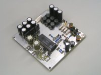
First photograph shows the component side. The 14 TDA1541A SMD film decoupling caps (1206 size) are located underneath the chip like with the previous design.
I used plain voltage regulators plus LC filtering, did some tests with shunt regs like TL431 but sound appeared to be less accurate. Anyway, separate shunt regulator modules can be used instead of the voltage regulators if required.
I/V resistors are moved away from the masterclock in order to minimize crosstalk with 11.2896 MHz.
Schottky diodes are used for DJA circuits, DEM synchronizer and BCK/WS attenuators.
The two selected JFETs (near I/V resistors) are used as current buffers. gate is tied to GND, so both, reference voltages and reference voltage filters could be removed. Interference from these reference voltages is now eliminated. The JFETs are selected for low Ugs in order to meet +/-25mV DC output compliance.
There is room for 4 optional JFETs that form unity gain buffers to isolate passive I/V resistor from external loads.
4-crystal masterclock is now integrated on the PCB, simplifying design. I added a DJA circuit between masterclock and BCK reclocker. The masterclock can be set to exactly 11.28960 MHz with a trimmer.
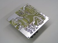
Second photograph shows the solder side. Here I put most of the SMD parts like resistors and decoupling caps. I used fastest available (5V) D flip-flop for BCK reclocking and driving the balanced DEM synchronizer.
The BCK D flip-flop is a tiny US8 size flip-flop with balanced outputs (Q /Q). Both WS and DATA are also synchronously reclocked using 2 more miniature SMD D flip-flops.
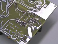
Third photograph shows a close-up of the tiny D flip-flops. It takes a steady hand and magnifying glass to solder these. The BCK D flip-flop measures approx. 2 x 3mm including the 8 terminals.
Hi all,
Project update.
The TDA1541A DAC module was redesigned, based on feedback from audiophiles. The objective was integrating all separate modules and solving some minor issues with sound quality.
I integrated following circuits on a single PCB:
-TDA1541A DAC chip + decoupling
-4 crystal masterclock
-BCK synchronous reclockers
-WS/DATA synchronous reclockers
-DEM synchronizer
-Voltage regulators
-Passive I/V converter with single JFET current buffer
-Unity gain output buffers
I attached some photographs of this new module.
First photograph shows the component side. The 14 TDA1541A SMD film decoupling caps (1206 size) are located underneath the chip like with the previous design.
I used plain voltage regulators plus LC filtering, did some tests with shunt regs like TL431 but sound appeared to be less accurate. Anyway, separate shunt regulator modules can be used instead of the voltage regulators if required.
I/V resistors are moved away from the masterclock in order to minimize crosstalk with 11.2896 MHz.
Schottky diodes are used for DJA circuits, DEM synchronizer and BCK/WS attenuators.
The two selected JFETs (near I/V resistors) are used as current buffers. gate is tied to GND, so both, reference voltages and reference voltage filters could be removed. Interference from these reference voltages is now eliminated. The JFETs are selected for low Ugs in order to meet +/-25mV DC output compliance.
There is room for 4 optional JFETs that form unity gain buffers to isolate passive I/V resistor from external loads.
4-crystal masterclock is now integrated on the PCB, simplifying design. I added a DJA circuit between masterclock and BCK reclocker. The masterclock can be set to exactly 11.28960 MHz with a trimmer.
Second photograph shows the solder side. Here I put most of the SMD parts like resistors and decoupling caps. I used fastest available (5V) D flip-flop for BCK reclocking and driving the balanced DEM synchronizer.
The BCK D flip-flop is a tiny US8 size flip-flop with balanced outputs (Q /Q). Both WS and DATA are also synchronously reclocked using 2 more miniature SMD D flip-flops.
Third photograph shows a close-up of the tiny D flip-flops. It takes a steady hand and magnifying glass to solder these. The BCK D flip-flop measures approx. 2 x 3mm including the 8 terminals.
Attachments
Hi ecdesigns,
I have been a silent admirer of both your innovative design ideas and of your perfectionist design philosophy. Your degree of passion for the advancement of music reproduction is quite evident, and I salute your efforts. I wonder if you might address the following two question regarding your DAC designs?
1. Among your many detailed design comments within this thread I don't recall reading your opinion regarding the in-band H.F. roll-off effect inherent to most all NOS DACs. From the description of your TDA1541A DAC module's output stage topology it appears that you have decided not to equalize that H.F. roll-off. Would you please comment on the reasoning by which you arrived at that apparent decision?
2. Regarding your apparent decision to utilize common 3-terminal 780x type voltage regulators followed by LC filtering to remove regulator noise, it would seem that the difficult to passively filter low-frequency regulator noise would increase the low-frequency jitter that you have taken such extreme pains to otherwise reduce. Would you please comment?
Best regards.
You have neglected the output buffer and supply regulation circuitry needed to ensure that your three component equalizer actually meets it's target response into the various interconnects and terminal loads to which it might be connected.
No buffer, no supply, but low impedance output.
-Passive I/V converter with single JFET current buffer
A passive I/V with a JFET is no passive I/V anymore.
Bernhard, your response is too terse to clearly understand exactly what your point is.No buffer, no supply, but low impedance output.
My point is that your example three component equalizer - an LCR bandpass filter, no doubt - would require an output isolation buffer circuit to ensure that neither interconnect capacitance nor terminal load impedance alters the target filter response, otherwise, why bother with an equalizer in the first place?
Secondly, an LCR bandpass filter is a resonant tank circuit having both a capacitor and an inductor, yes? Is there really any debate today that capacitors and inductors can alter perceived sound quality.
Given those points, I don't see how you rather cavalierly dismiss the notion that such an equalizer circuit has the potential to harm perceived audio transparency, buffer or none.
Hi Bernhard,
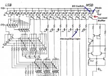
I attached part of TDA1541A schematics.
I marked bit switch, diode and current buffer. Bit currents from 10 MSBs are buffered using on-chip current buffers (marked with red arrow). Buffered current is either routed to +5V (diode conducts / bit is not used), or to the output (bit switch transistor conducts, diode does not conduct).
What I did is simply add another external current buffer that presents a low impedance to the DAC output (compliance) and provides an output that's no longer limited by DAC output compliance. I used a single selected JFET for this. The JFET gate current is specified at 1nA, LSB bit current equals 61nA. So DAC output current is simply passed by this JFET current buffer.
Actual I/V conversion takes place in a 500R passive I/V resistor. Big difference with most passive I/V converters for TDA1541A is that this one generates 2Vpp directly across the I/V resistor with no need for active amplification. This keeps noise levels down and provides required large bandwidth to cope with TDA1541A output spectrum.
A passive I/V with a JFET is no passive I/V anymore.
I attached part of TDA1541A schematics.
I marked bit switch, diode and current buffer. Bit currents from 10 MSBs are buffered using on-chip current buffers (marked with red arrow). Buffered current is either routed to +5V (diode conducts / bit is not used), or to the output (bit switch transistor conducts, diode does not conduct).
What I did is simply add another external current buffer that presents a low impedance to the DAC output (compliance) and provides an output that's no longer limited by DAC output compliance. I used a single selected JFET for this. The JFET gate current is specified at 1nA, LSB bit current equals 61nA. So DAC output current is simply passed by this JFET current buffer.
Actual I/V conversion takes place in a 500R passive I/V resistor. Big difference with most passive I/V converters for TDA1541A is that this one generates 2Vpp directly across the I/V resistor with no need for active amplification. This keeps noise levels down and provides required large bandwidth to cope with TDA1541A output spectrum.
Attachments
Hello EC, is your new JFET approach much better than this schematic also posted by you?
can you show what values needs to be modified here in order to have 2Vrms at the output and not 2Vpp?
you said in an earlier post that after extensive tests you decided not to reclock WS and Data lines, is it proven now to be better also recklocking these 2 lines? those 2 extra flip flops don't they add extra jitter being aditional clock loads?
you also say in your updated project that you use "D flip-flop for BCK reclocking and driving the balanced DEM synchronizer." - do you use now both flip flop outputs to drive the dem circuit? cause before i remember you saying that just 1 pin is used feeding it through a 13k resistor and a diode and the other is left unconnected
Thanks
An externally hosted image should be here but it was not working when we last tested it.
can you show what values needs to be modified here in order to have 2Vrms at the output and not 2Vpp?
you said in an earlier post that after extensive tests you decided not to reclock WS and Data lines, is it proven now to be better also recklocking these 2 lines? those 2 extra flip flops don't they add extra jitter being aditional clock loads?
you also say in your updated project that you use "D flip-flop for BCK reclocking and driving the balanced DEM synchronizer." - do you use now both flip flop outputs to drive the dem circuit? cause before i remember you saying that just 1 pin is used feeding it through a 13k resistor and a diode and the other is left unconnected
Thanks
Last edited:
Hi Ken newton,
1) I use large bandwidth signal processing up to the speakers. The step-shaped signal at higher frequencies provides more energy at these frequencies compared to sinewave shape. This provides some compensation for trebles roll-off. Fine tuning was made by correcting tweeter attenuation factor in the speaker crossover filter.
2) How are most linear IC regulators used? bridge rectifier > smoothing cap > IC regulator. This way the regulator receives a DC voltage with ripple voltage, rectifier switching noise and mains interference. IC Regulator feedback loop bandwidth is usually limited to approx. 10 KHz. So it's not surprising that this provides poor results.
I started with a 3-stage stepped rectifier that greatly reduces rectifier switching noise. Next I use a capacitance multiplier that reduces ripple voltage and noise to approx. 1mVpp. This clean DC voltage then passes a LC filter before it arrives at the regulator. Regulator noise is filtered by a LC filter placed after the regulator.
Sensitive circuits like masterclock and bit reclocker are powered through an extra 6th order LC filter in order to further reduce noise. Masterclock was designed to offer up to 40 times better PSRR compared to conventional Colpitts oscillators. This was achieved by using multiple crystals, no phase shifting caps and complementary JFET buffers that compensate for the effect of voltage induced capacitance fluctuations.
The TDA1541A-MK2 module masterclock consists of 4 crystals, one trimmer, complementary JFET pair, and a choke.
Hi luxury54,
Perceived sound quality has improved a lot. There is less "stress" in the sound and sound is smoother / cleaner.
The filtered reference voltage is no longer needed as the JFET gate (current buffer) now connects to GND. The DC voltage on the TDA1541A output was trimmed by using selected JFETs.
The JFET gate current is specified at 1nA, this is much lower compared to LSB bit current of 61nA. So the JFET simply passes the DAC current without adding significant drive current like with the Darlington circuit. JFET property is the ability to conduct current without applying drive voltage (Ugs = 0V).
R2 = (2*SQRT(2)*2)/0.04) = 1414 Ohm, or 1K5 (closest E12 value). This will then produce 1500 * 0.004 = 6Vpp. Higher supply voltage (9V DC for example) is required to prevent clipping.
Correct, so I didn't connect these WS and DATA reclockers to the masterclock output. I used a buffered 5.6554 MHz clock from the display controller instead.
Clock distribution now is as follows:
BCK: Masterclock > DJA > bit reclocker > DJA.
DEM: Masterclock > DJA > bit reclocker.
Display controller: Masterclock > clock buffer.
DATA / WS reclockers: Masterclock > clock buffer > divider / buffer (display controller).
DSP: Masterclock > clock buffer > divider / buffer (display controller).
masterclock drives 2 clock loads, BCK reclocker and clock buffer. BCK reclocker was connected directly to the masterclock in order to prevent cumulative jitter (clock buffers).
The audible effect of WS and DATA reclockers are improved bass and cleaner sound. This illustrates that all I2S signals affect sound quality, not only the timing signals BCK or WS).
Yes I use both BCK reclocker outputs (Q and /Q) to synchronize the DEM oscillator now. Pin 16 and pin 17 are tied to -15V using two 2K2 resistors, this prevents the DEM oscillator from oscillating on stray capacitance. Balanced signal is injected on pin 16 (/Q) and 17 (Q) using a BAT42 Schottky diode in series with a 12K resistor.
Hello EC, is your new JFET approach much better than this schematic also posted by you?
Perceived sound quality has improved a lot. There is less "stress" in the sound and sound is smoother / cleaner.
The filtered reference voltage is no longer needed as the JFET gate (current buffer) now connects to GND. The DC voltage on the TDA1541A output was trimmed by using selected JFETs.
The JFET gate current is specified at 1nA, this is much lower compared to LSB bit current of 61nA. So the JFET simply passes the DAC current without adding significant drive current like with the Darlington circuit. JFET property is the ability to conduct current without applying drive voltage (Ugs = 0V).
can you show what values needs to be modified here in order to have 2Vrms at the output and not 2Vpp?
R2 = (2*SQRT(2)*2)/0.04) = 1414 Ohm, or 1K5 (closest E12 value). This will then produce 1500 * 0.004 = 6Vpp. Higher supply voltage (9V DC for example) is required to prevent clipping.
you said in an earlier post that after extensive tests you decided not to reclock WS and Data lines, is it proven now to be better also recklocking these 2 lines? those 2 extra flip flops don't they add extra jitter being aditional clock loads?
Correct, so I didn't connect these WS and DATA reclockers to the masterclock output. I used a buffered 5.6554 MHz clock from the display controller instead.
Clock distribution now is as follows:
BCK: Masterclock > DJA > bit reclocker > DJA.
DEM: Masterclock > DJA > bit reclocker.
Display controller: Masterclock > clock buffer.
DATA / WS reclockers: Masterclock > clock buffer > divider / buffer (display controller).
DSP: Masterclock > clock buffer > divider / buffer (display controller).
masterclock drives 2 clock loads, BCK reclocker and clock buffer. BCK reclocker was connected directly to the masterclock in order to prevent cumulative jitter (clock buffers).
The audible effect of WS and DATA reclockers are improved bass and cleaner sound. This illustrates that all I2S signals affect sound quality, not only the timing signals BCK or WS).
you also say in your updated project that you use "D flip-flop for BCK reclocking and driving the balanced DEM synchronizer." - do you use now both flip flop outputs to drive the dem circuit? cause before i remember you saying that just 1 pin is used feeding it through a 13k resistor and a diode and the other is left unconnected
Yes I use both BCK reclocker outputs (Q and /Q) to synchronize the DEM oscillator now. Pin 16 and pin 17 are tied to -15V using two 2K2 resistors, this prevents the DEM oscillator from oscillating on stray capacitance. Balanced signal is injected on pin 16 (/Q) and 17 (Q) using a BAT42 Schottky diode in series with a 12K resistor.
Hello ecdesigns,
it would be very nice to have a look at the schematic of this new version of the TDA1541 based dac. At least at the parts regarding the output stage and the ultimate DEM reclock. Please, please...
Best regards.
Paul
it would be very nice to have a look at the schematic of this new version of the TDA1541 based dac. At least at the parts regarding the output stage and the ultimate DEM reclock. Please, please...
Best regards.
Paul
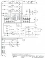
TDA1541A-MK2 module schematics.
Hi Sandor,
I attached TDA1541A-MK2 module full schematics (non-commercial use only).
+10V, -10V, and -20V outputs from the capacitance multipliers on the power supply module are LC filtered (N3 .. N5, FB1 ... FB3, C31 ... C33, C17, C20, C23). Voltage regulators are used to derive +5V, -5V, and -15V. Voltage regulator outputs are connected to large value electrolytic caps (C34 ... C36) to attenuate regulator noise. LC filters (FB4 ... FB6, C19, C22, C25) are used for extra filtering.
Additional 6th order LC filter (N6 ... N8, FB7, FB8, C38 ... C40) is used for master clock, clock buffer and bit reclocker. The DC resistance of chokes N6 ... N8 (approx. 60 Ohms in total) together with the connected loads result in approx. 4V output voltage. I used no regulators after this filter to keep noise levels down.
The 4-crystal master clock consists of X1 ... X4, C1, T3, T7, FB11, N1. T3 and T7 form a unity gain complementary buffer. Crystals are driven through combined gs capacitance of both JFETs. Phase shift is accomplished using choke N1. Output swings between -4V and +4V (8Vpp). Clock buffer (T4, T8, FB12, N2) is connected through R3. Source is driven through clock rectifier D9, R21, R4.
Bit reclocker (U5) is clocked through DJA1 (D8, D10, R2, R7, R12, C16), the DJA also acts as clock rectifier. Bit reclocker output is balanced (Q /Q). The Q output drives DJA2 (D3 ... D6, R1, R5, R6, C26). DJA2 drives the TDA1541A clock input.
The balanced output of DJA2 drives the DEM synchronizer (D6, D7, R22, R23, R19, R20). The DEM synchronizer drives the DEM oscillator through pin 16 and 17. Bit clock equals DEM clock (1.4112 MHz).
Decoupling caps (C2 ... C15) are 1206 size PPS SMD film caps with stacked construction (low inductance) and high insulation resistance (>3000 M Ohm).
Both WS and DATA are synchronously reclocked (U6 and U7) and fed to the TDA1541A using attenuators (D1, D2, R10, R11, R13, R14). These reclockers are powered by 3.3V and clocked with buffered 5.6448 MHz from the SD-transport.
TDA1541A output currents enter JFET current buffers T1 and T2 that pass the DAC current to passive I/V resistors R8 and R9. The JFET current buffers are required to meet DAC output compliance. The current buffer JFETs need to have high Yfs and need to be selected for lowest voltage on the DAC outputs. Gate current equals approx. 1nA while LSB current equals approx. 61nA.
Amplitude across 500 Ohm passive I/V resistors equals 2Vpp. This signal can be buffered (T5, T6, T9, T10) using optional complementary unity gain JFET buffers.
Hi Sandor,
it would be very nice to have a look at the schematic of this new version of the TDA1541 based dac.
I attached TDA1541A-MK2 module full schematics (non-commercial use only).
+10V, -10V, and -20V outputs from the capacitance multipliers on the power supply module are LC filtered (N3 .. N5, FB1 ... FB3, C31 ... C33, C17, C20, C23). Voltage regulators are used to derive +5V, -5V, and -15V. Voltage regulator outputs are connected to large value electrolytic caps (C34 ... C36) to attenuate regulator noise. LC filters (FB4 ... FB6, C19, C22, C25) are used for extra filtering.
Additional 6th order LC filter (N6 ... N8, FB7, FB8, C38 ... C40) is used for master clock, clock buffer and bit reclocker. The DC resistance of chokes N6 ... N8 (approx. 60 Ohms in total) together with the connected loads result in approx. 4V output voltage. I used no regulators after this filter to keep noise levels down.
The 4-crystal master clock consists of X1 ... X4, C1, T3, T7, FB11, N1. T3 and T7 form a unity gain complementary buffer. Crystals are driven through combined gs capacitance of both JFETs. Phase shift is accomplished using choke N1. Output swings between -4V and +4V (8Vpp). Clock buffer (T4, T8, FB12, N2) is connected through R3. Source is driven through clock rectifier D9, R21, R4.
Bit reclocker (U5) is clocked through DJA1 (D8, D10, R2, R7, R12, C16), the DJA also acts as clock rectifier. Bit reclocker output is balanced (Q /Q). The Q output drives DJA2 (D3 ... D6, R1, R5, R6, C26). DJA2 drives the TDA1541A clock input.
The balanced output of DJA2 drives the DEM synchronizer (D6, D7, R22, R23, R19, R20). The DEM synchronizer drives the DEM oscillator through pin 16 and 17. Bit clock equals DEM clock (1.4112 MHz).
Decoupling caps (C2 ... C15) are 1206 size PPS SMD film caps with stacked construction (low inductance) and high insulation resistance (>3000 M Ohm).
Both WS and DATA are synchronously reclocked (U6 and U7) and fed to the TDA1541A using attenuators (D1, D2, R10, R11, R13, R14). These reclockers are powered by 3.3V and clocked with buffered 5.6448 MHz from the SD-transport.
TDA1541A output currents enter JFET current buffers T1 and T2 that pass the DAC current to passive I/V resistors R8 and R9. The JFET current buffers are required to meet DAC output compliance. The current buffer JFETs need to have high Yfs and need to be selected for lowest voltage on the DAC outputs. Gate current equals approx. 1nA while LSB current equals approx. 61nA.
Amplitude across 500 Ohm passive I/V resistors equals 2Vpp. This signal can be buffered (T5, T6, T9, T10) using optional complementary unity gain JFET buffers.
Attachments
damn, this man is sharing all his knowledge with us based on his intensive time consuming experiments.
We should be very gratefull getting all this for free...I don't know many persons who would do this, although even in the bible it is written that knowledge worths nothing if is not shared among people coming in the benefit of all mankind...
Big thanks EC !
We should be very gratefull getting all this for free...I don't know many persons who would do this, although even in the bible it is written that knowledge worths nothing if is not shared among people coming in the benefit of all mankind...
Big thanks EC !
Last edited:
I think the bible was referring to the PCM63.
Probably, but the prophet of PCM63 is silent for more than 2000 years 😉
Now, if you would share the knowledge it would make you and the mankind a lot better! 🙂
Cheers,
M.
re diagram on post 3335
Hi John,
Many thanks for the diagram - helps a lot.
Pardon my ignorance, this has probably been covered ages ago but on the cct diagram, the pin 4 of the 1541A dac chip is connected directly to pin5 (gnd) rather than the usual pin2 (BCK) - could you say why and if it only applies to your system or can be useful in more "standard" application?
- Home
- Source & Line
- Digital Line Level
- Building the ultimate NOS DAC using TDA1541A