Hi oshifis,
One year ago I would say, yes, reclocking BCK is enough (for DAC chips that use BCK as timing reference for latching the outputs).
But now it seems like all I2S signals that contain timing jitter will couple this jitter into the DAC chip and might affect sound quality. Spectrum analysis still shows source jitter signature in the DAC output signal after synchronous reclocking of the timing signal.
Each I2S signal, DATA, WS, and BCK basically consists of a bunch of sine waves. The square wave WS signal consists of the fundamental (44.1 KHz for example) and higher harmonics, same applies for DATA and BCK.
This basically means that by injecting these I2S signals into the DAC chip, all higher harmonics are injected too. So if any of the I2S signals contains jitter, it will be coupled into the DAC electronics and will affect the DAC output signal.
The easiest way to reduce this effect a little bit, is using I2S attenuators, and use reclocking on all I2S signals. Note that its very difficult to fully block source jitter, it will always seep through to some extent (crosstalk / EMI).
Other issue is master clock jitter (after connecting all loads). Master clock jitter performance is directly affected by connected loads (even crosstalk through clock buffers), especially when these capacitive loads aren't absolutely constant. One can test this by connecting the master clock to a frequency counter and measure the exact clock frequency with and without capacitive load (say 47pF). The frequency will vary, thus varying load capacitance (capacitance modulation) could lead to varying master clock frequency or jitter.
Clock buffers and comparators add jitter too, and the stray capacitance between both input and output will couple connected loads to the master clock output.
so it would be best not to use any if possible.
This means that the master clock needs to have sufficient output power to directly drive a number of (capacitive) clock loads without requiring clock buffers, and the output signal transient(s) are steep enough to reliably trigger connected logic.
Given the load capacitance fluctuations at specific frequencies, its best to keep highest clock frequency present in the DAC chip as low as possible, since these small capacitance fluctuations will have biggest impact on higher (clock) frequencies.
Thats one of the reasons I reverted to minimum possible clock frequencies in the SD-player, by running the DAC chip on a 1.4112 MHz bit clock. Systems with higher sample rates (and required higher clock frequencies) are more likely to be affected by these varying (load) capacitances. This could lead to increased clock jitter levels at higher sample rates.
The TDA1541A could even be driven in simultaneous mode (pin 27 tied to -5V) allowing for lowest bit clock frequency of 705.6 KHz.
Why is it necessary to reclock the DATA and WS signals? Reclocking BCK wouldn't be enough?
One year ago I would say, yes, reclocking BCK is enough (for DAC chips that use BCK as timing reference for latching the outputs).
But now it seems like all I2S signals that contain timing jitter will couple this jitter into the DAC chip and might affect sound quality. Spectrum analysis still shows source jitter signature in the DAC output signal after synchronous reclocking of the timing signal.
Each I2S signal, DATA, WS, and BCK basically consists of a bunch of sine waves. The square wave WS signal consists of the fundamental (44.1 KHz for example) and higher harmonics, same applies for DATA and BCK.
This basically means that by injecting these I2S signals into the DAC chip, all higher harmonics are injected too. So if any of the I2S signals contains jitter, it will be coupled into the DAC electronics and will affect the DAC output signal.
The easiest way to reduce this effect a little bit, is using I2S attenuators, and use reclocking on all I2S signals. Note that its very difficult to fully block source jitter, it will always seep through to some extent (crosstalk / EMI).
Other issue is master clock jitter (after connecting all loads). Master clock jitter performance is directly affected by connected loads (even crosstalk through clock buffers), especially when these capacitive loads aren't absolutely constant. One can test this by connecting the master clock to a frequency counter and measure the exact clock frequency with and without capacitive load (say 47pF). The frequency will vary, thus varying load capacitance (capacitance modulation) could lead to varying master clock frequency or jitter.
Clock buffers and comparators add jitter too, and the stray capacitance between both input and output will couple connected loads to the master clock output.
so it would be best not to use any if possible.
This means that the master clock needs to have sufficient output power to directly drive a number of (capacitive) clock loads without requiring clock buffers, and the output signal transient(s) are steep enough to reliably trigger connected logic.
Given the load capacitance fluctuations at specific frequencies, its best to keep highest clock frequency present in the DAC chip as low as possible, since these small capacitance fluctuations will have biggest impact on higher (clock) frequencies.
Thats one of the reasons I reverted to minimum possible clock frequencies in the SD-player, by running the DAC chip on a 1.4112 MHz bit clock. Systems with higher sample rates (and required higher clock frequencies) are more likely to be affected by these varying (load) capacitances. This could lead to increased clock jitter levels at higher sample rates.
The TDA1541A could even be driven in simultaneous mode (pin 27 tied to -5V) allowing for lowest bit clock frequency of 705.6 KHz.
Hi maxlorenz,
Digikey PN 296-9852-1-ND
SN74LVC1G80 series SOT23-5 (SMD), inverted Q output.
Digikey PN 296-9849-1-ND
SN74LVC1G79 series SOT23-5 (SMD), Non-inverted Q output.
When using an interpolator, the resulting output signal will change when the bit clock (BCK) changes from LOW to HIGH level as the 74HC164 triggers on the positive going edge of BCK.
DAC chips like the TDA1541A and TDA1543 samples input data during the positive going edge of BCK too. This means that when the DAC chip does not receive an inverted BCK clock signal, it will attempt to sample on the exact moment the SN74HC164 outputs are changing (since both 74HC164 and DAC chip trigger on the same moment.
By inverting the DAC chip bit clock, the DAC chip will sample the 74HC164 output signal after it has settled (1/2 BCK delay), ensuring reliable sampling of the I2S data provided by the interpolator circuit.
If the first DAC chip was connected directly to the I2S source (no delay), while the remaining DAC chips were connected to the interpolator, this would mean that the first DAC chip would require non-inverted bit clock, and the remaining DAC chips an inverted bit clock.
By connecting all DAC chips to the interrpolator, introducing an additional delay for all outputs, all DAC chips can now be triggered using an inverted bit clock, thus outputting samples at exactly the same moment.
Example:
No delay for first DAC chip, DAC # 2,3 and 4 trigger half BCK period time after DAC #1 triggers.
DAC #1, no delay, non-inverted bit clock
DAC #2, 32 BCK delay, inverted bit clock
DAC #3, 16 BCK delay, inverted bit clock
DAC #4, 24 BCK delay, inverted bit clock
All DAC chips receiving delayed I2S signals, all DAC chips trigger at the same time.
DAC #1, 1 BCK delay, inverted bit clock
DAC #2, 33 BCK delay, inverted bit clock
DAC #3, 17 BCK delay, inverted bit clock
DAC #4, 25 BCK delay, inverted bit clock
Would you care to mention suitable high speed D flip-flop...that would be on Digikey's catalog?
Digikey PN 296-9852-1-ND
SN74LVC1G80 series SOT23-5 (SMD), inverted Q output.
Digikey PN 296-9849-1-ND
SN74LVC1G79 series SOT23-5 (SMD), Non-inverted Q output.
The inverted Clock puzzles me, though...
When using an interpolator, the resulting output signal will change when the bit clock (BCK) changes from LOW to HIGH level as the 74HC164 triggers on the positive going edge of BCK.
DAC chips like the TDA1541A and TDA1543 samples input data during the positive going edge of BCK too. This means that when the DAC chip does not receive an inverted BCK clock signal, it will attempt to sample on the exact moment the SN74HC164 outputs are changing (since both 74HC164 and DAC chip trigger on the same moment.
By inverting the DAC chip bit clock, the DAC chip will sample the 74HC164 output signal after it has settled (1/2 BCK delay), ensuring reliable sampling of the I2S data provided by the interpolator circuit.
If the first DAC chip was connected directly to the I2S source (no delay), while the remaining DAC chips were connected to the interpolator, this would mean that the first DAC chip would require non-inverted bit clock, and the remaining DAC chips an inverted bit clock.
By connecting all DAC chips to the interrpolator, introducing an additional delay for all outputs, all DAC chips can now be triggered using an inverted bit clock, thus outputting samples at exactly the same moment.
Example:
No delay for first DAC chip, DAC # 2,3 and 4 trigger half BCK period time after DAC #1 triggers.
DAC #1, no delay, non-inverted bit clock
DAC #2, 32 BCK delay, inverted bit clock
DAC #3, 16 BCK delay, inverted bit clock
DAC #4, 24 BCK delay, inverted bit clock
All DAC chips receiving delayed I2S signals, all DAC chips trigger at the same time.
DAC #1, 1 BCK delay, inverted bit clock
DAC #2, 33 BCK delay, inverted bit clock
DAC #3, 17 BCK delay, inverted bit clock
DAC #4, 25 BCK delay, inverted bit clock
But isn't this what the clock buffers are meant to do - buffer the clock from the fluctuations of the outside world - you seem to have reversed this idea?Other issue is master clock jitter (after connecting all loads). Master clock jitter performance is directly affected by connected loads (even crosstalk through clock buffers), especially when these capacitive loads aren't absolutely constant. One can test this by connecting the master clock to a frequency counter and measure the exact clock frequency with and without capacitive load (say 47pF). The frequency will vary, thus varying load capacitance (capacitance modulation) could lead to varying master clock frequency or jitter.
Clock buffers and comparators add jitter too, and the stray capacitance between both input and output will couple connected loads to the master clock output.
so it would be best not to use any if possible.
This means that the master clock needs to have sufficient output power to directly drive a number of (capacitive) clock loads without requiring clock buffers, and the output signal transient(s) are steep enough to reliably trigger connected logic.
That sounds like a good idea (following your logic), why didn't you implement this?The TDA1541A could even be driven in simultaneous mode (pin 27 tied to -5V) allowing for lowest bit clock frequency of 705.6 KHz.
Dear EC,
Many thanks for your reply. (post nº 3042)
Unfortunately, SMD is hard for me. I understand that I can use 74HC164 not as interpolator but as reclocker, due to the Dflip-flop capacity, one for each I2S signal, using the same delay for each one (say 1BCK), but I have to figure how to get inverted clock...I'll have to study the datasheet further...
Yesterday I successfully completed the attenuator for WS and the dynamic jitter attenuator for BCK. I used the stock schematic that you provided for the DJA of your lossless player, with 200nf//variable R to get 1,2VDC at the BCK input. I never got the "lowest ripple possible" thing. If I read between 150R and "490R" (variable R in my case) the ripple is a function of 150R, not of the paralelled capacitor...(?)
It sounds quite better. 😎
I will try my little 4DAC tower... 😉
Cheers,
M
Dear John,
I checked the chips you recommended>
From a mechanical point of view I think it is highly possible to do it!
If I understood correctly your explanation, I must use the inverting Q flip flop for BCK and the non inverting for DATA and WS, right?
Regards,
M
I checked the chips you recommended>
Quote:
Would you care to mention suitable high speed D flip-flop...that would be on Digikey's catalog?
Digikey PN 296-9852-1-ND
SN74LVC1G80 series SOT23-5 (SMD), inverted Q output.
Digikey PN 296-9849-1-ND
SN74LVC1G79 series SOT23-5 (SMD), Non-inverted Q output.
From a mechanical point of view I think it is highly possible to do it!
If I understood correctly your explanation, I must use the inverting Q flip flop for BCK and the non inverting for DATA and WS, right?
Regards,
M
Thats one of the reasons I reverted to minimum possible clock frequencies in the SD-player, by running the DAC chip on a 1.4112 MHz bit clock. Systems with higher sample rates (and required higher clock frequencies) are more likely to be affected by these varying (load) capacitances. This could lead to increased clock jitter levels at higher sample rates.
The TDA1541A could even be driven in simultaneous mode (pin 27 tied to -5V) allowing for lowest bit clock frequency of 705.6 KHz.
Great advice on reducing the "digital artifacts" in the analog system.
jk
Hi EC,
How did you drive the TDA in simultaneous mode? The SAA7210/7220 can not output anything but I2S. Or dou you have some "trick"?
I could build in a TDA1541A in a Marantz CD-84 (no I2S signal) and drive from the original SAA7000, NOS mode. It had 2xTDA1540P originally.
How did you drive the TDA in simultaneous mode? The SAA7210/7220 can not output anything but I2S. Or dou you have some "trick"?
I could build in a TDA1541A in a Marantz CD-84 (no I2S signal) and drive from the original SAA7000, NOS mode. It had 2xTDA1540P originally.
Hello
Does anyone know the answer of my little doubt?
I'm planning to make a CD player with Philips CD-PRO2LF and TDA1541A.
Can the i2s output from CD-PRO2LF operate TDA1541A without trouble?
I do not know so about digital audio.It's my first plan to make CDP.
Thank you
Does anyone know the answer of my little doubt?
I'm planning to make a CD player with Philips CD-PRO2LF and TDA1541A.
Can the i2s output from CD-PRO2LF operate TDA1541A without trouble?
I do not know so about digital audio.It's my first plan to make CDP.
Thank you
Hello
Does anyone know the answer of my little doubt?
I'm planning to make a CD player with Philips CD-PRO2LF and TDA1541A.
Can the i2s output from CD-PRO2LF operate TDA1541A without trouble?
I do not know so about digital audio.It's my first plan to make CDP.
Thank you
Yes I use the CD-Pro2 LF with the TD1541A via the I2S output of the CD-Pro.
jk
Thank you for reply jstang.
Your answer gave me big courage.
It was uneasy whether to accept the output of latest CDpro2LF because TDA141A is "vintage" parts.
Thanks again!
Your answer gave me big courage.
It was uneasy whether to accept the output of latest CDpro2LF because TDA141A is "vintage" parts.
Thanks again!
Hi jkeny,
Clock buffers are primarily intended for increasing circuit fan-out, meaning the buffered signal can now drive more (TTL) loads.
Buffers increase timing jitter, the more (cascaded) clock buffers, the higher the jitter.
If there is a coupling capacitance between clock buffer input and output, the buffer will fail to completely isolate the (master) clock from capacitive load fluctuations at the clock buffer output.
The clock buffer will also have a certain input capacitance that may not be constant over a wide frequency range. This will then lead to connected (master) clock frequency fluctuations too.
Thats why I use a 3-crystal clock with power output in the SD-player as it doesn't require clock buffers to drive multiple loads. The design is also optimized for maintaining extreme low jitter levels despite frequency dependent load capacitance fluctuations.
It's not that simple, possible solution might look like this:
I2S DATA (L + R sample) is clocked into a RAM buffer using 1.4112 MHz bit clock. This would require 32 bit clocks. When both left and right samples are received, they are clocked out simultaneously using 705.6 KHz bit clock. This would take 16 bit clocks at half the bit clock frequency. during this time the new samples (L + R) are clocked into the RAM buffer.
Anyway, the TDA1541A would have to run on battery power in order to make a chance to outperform the TDA1543 running on a clean battery power supply. The I/V converter would have to be fully passive too, as adding a single semiconductor in the signal path would already result in poorer performance compared with the TDA1543 in the SD-player that only uses passive I/V conversion.
But, when using balanced outputs, and manipulate TDA1541A output compliance using a passive split I/V resistor with bias current (resistor to +5V), it would be possible to squeeze up to approx. 2 x 550mVpp out of these chips. This would be more than enough to drive the latest balanced input FET bridge power amp into clipping.
But isn't this what the clock buffers are meant to do - buffer the clock from the fluctuations of the outside world - you seem to have reversed this idea?
Clock buffers are primarily intended for increasing circuit fan-out, meaning the buffered signal can now drive more (TTL) loads.
Buffers increase timing jitter, the more (cascaded) clock buffers, the higher the jitter.
If there is a coupling capacitance between clock buffer input and output, the buffer will fail to completely isolate the (master) clock from capacitive load fluctuations at the clock buffer output.
The clock buffer will also have a certain input capacitance that may not be constant over a wide frequency range. This will then lead to connected (master) clock frequency fluctuations too.
Thats why I use a 3-crystal clock with power output in the SD-player as it doesn't require clock buffers to drive multiple loads. The design is also optimized for maintaining extreme low jitter levels despite frequency dependent load capacitance fluctuations.
That sounds like a good idea (following your logic), why didn't you implement this?
It's not that simple, possible solution might look like this:
I2S DATA (L + R sample) is clocked into a RAM buffer using 1.4112 MHz bit clock. This would require 32 bit clocks. When both left and right samples are received, they are clocked out simultaneously using 705.6 KHz bit clock. This would take 16 bit clocks at half the bit clock frequency. during this time the new samples (L + R) are clocked into the RAM buffer.
Anyway, the TDA1541A would have to run on battery power in order to make a chance to outperform the TDA1543 running on a clean battery power supply. The I/V converter would have to be fully passive too, as adding a single semiconductor in the signal path would already result in poorer performance compared with the TDA1543 in the SD-player that only uses passive I/V conversion.
But, when using balanced outputs, and manipulate TDA1541A output compliance using a passive split I/V resistor with bias current (resistor to +5V), it would be possible to squeeze up to approx. 2 x 550mVpp out of these chips. This would be more than enough to drive the latest balanced input FET bridge power amp into clipping.
Hi maxlorenz,
First adjust R to obtain approx. 1.2V DC. Then leave it at this value.
next increase 200nF capacitance, observing ripple amplitude on the capacitor. use steps of 100nF until ripple voltage starts to drop, then fine-tune using smaller values until lowest ripple voltage is obtained. With low R (150 Ohm for example) capacitance has to be increased significantly before the ripple voltage starts to drop, you could end up with values in the uF range.
This adjustment is critical, the circuit will only work as planned when correctly tuned.
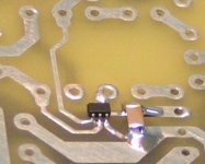
use a piece of printed circuit board and create some isolated pads using a fine saw. Then solder the SOT-23 part on these pads, this way its much easier to experiment with these devices. The flip-flop in the SD-player is even smaller size (I added a photograph), the capacitor next to it is 1206 size).
If I understood correctly your explanation, I must use the inverting Q flip flop for BCK and the non inverting for DATA and WS, right?[/quote]
yes you could do that, BCK then connects to the D inputs of both flip flops. the master clock connects to both flip-flop clock inputs. The flip-flop outputs would then provide both inverted and non-inverted BCK signals while maintaining low jitter. But make sure to connect the D flip-flops to very clean power supplies, you could use the posted SD-player schematics as reference for this.
I never got the "lowest ripple possible" thing. If I read between 150R and "490R" (variable R in my case) the ripple is a function of 150R, not of the paralelled capacitor...(?)
First adjust R to obtain approx. 1.2V DC. Then leave it at this value.
next increase 200nF capacitance, observing ripple amplitude on the capacitor. use steps of 100nF until ripple voltage starts to drop, then fine-tune using smaller values until lowest ripple voltage is obtained. With low R (150 Ohm for example) capacitance has to be increased significantly before the ripple voltage starts to drop, you could end up with values in the uF range.
This adjustment is critical, the circuit will only work as planned when correctly tuned.
From a mechanical point of view I think it is highly possible to do it!
use a piece of printed circuit board and create some isolated pads using a fine saw. Then solder the SOT-23 part on these pads, this way its much easier to experiment with these devices. The flip-flop in the SD-player is even smaller size (I added a photograph), the capacitor next to it is 1206 size).
If I understood correctly your explanation, I must use the inverting Q flip flop for BCK and the non inverting for DATA and WS, right?[/quote]
yes you could do that, BCK then connects to the D inputs of both flip flops. the master clock connects to both flip-flop clock inputs. The flip-flop outputs would then provide both inverted and non-inverted BCK signals while maintaining low jitter. But make sure to connect the D flip-flops to very clean power supplies, you could use the posted SD-player schematics as reference for this.
Attachments
Thanks EC, for your reply.
I already have 1.2V. When you say "ripple amplitude ON the capacitor", where exactly do you mean I must measure?
Do I measure across the capacitor?
I will send you a diagram before doing it... 😉
Regards,
M
First adjust R to obtain approx. 1.2V DC. Then leave it at this value.
next increase 200nF capacitance, observing ripple amplitude on the capacitor. use steps of 100nF until ripple voltage starts to drop, then fine-tune using smaller values until lowest ripple voltage is obtained. With low R (150 Ohm for example) capacitance has to be increased significantly before the ripple voltage starts to drop, you could end up with values in the uF range.
I already have 1.2V. When you say "ripple amplitude ON the capacitor", where exactly do you mean I must measure?
Do I measure across the capacitor?
yes you could do that, BCK then connects to the D inputs of both flip flops. the master clock connects to both flip-flop clock inputs. The flip-flop outputs would then provide both inverted and non-inverted BCK signals while maintaining low jitter. But make sure to connect the D flip-flops to very clean power supplies, you could use the posted SD-player schematics as reference for this.
I will send you a diagram before doing it... 😉
Regards,
M
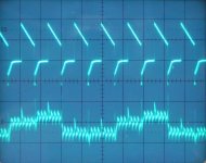
Hi maxlorenz,
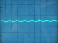
Yes, that's correct, the ripple voltage is measured across the capacitor.
I attached some oscillograms, first one shows the remaining ripple voltage across the capacitor after tuning. Setting: 10mV / div (using 1:10 probe), time div, 0.5uS / div (ripple voltage frequency equals 1.4112 MHz).
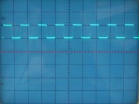
I also attached an oscillogram of the clock output signal of the DJA, 1V/div, red line marks 0V DC.
I already have 1.2V. When you say "ripple amplitude ON the capacitor", where exactly do you mean I must measure?
Do I measure across the capacitor?
Yes, that's correct, the ripple voltage is measured across the capacitor.
I attached some oscillograms, first one shows the remaining ripple voltage across the capacitor after tuning. Setting: 10mV / div (using 1:10 probe), time div, 0.5uS / div (ripple voltage frequency equals 1.4112 MHz).
I also attached an oscillogram of the clock output signal of the DJA, 1V/div, red line marks 0V DC.
Attachments
Hi fastvideo,
This is probably caused by the waveform at these pins (frequency counter doesn't trigger correctly).
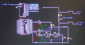
The exact on-chip DEM clock frequency, and correct operation of the on-chip DEM circuits can be measured at one of the decoupling pins (active divider output) with the 100nF decoupling cap removed.
The frequency can be determined by observing the intervals between the small amplitude changes. I attached an oscillogram showing both the external DEM clock signal and the resulting signal on one of the decoupling pins with the 100nF decoupling cap removed (lower trace). The active divider averaging circuit switches at the negative going edge of the external DEM clock. The step-shaped signal at the decoupling pin (active divider output) is caused by tolerances in the preceding passive divider that's based on emitter scaling.
The bit clock interference (2.8224 MHz in this case) is also clearly visible. That's why it's so important to sync the DEM clock with the bit clock. If the DEM clock is not synced with the bit clock (data sheet application) both bit clock and free running DEM oscillator frequency will inter modulate on the chip.
It's also important to make sure the active divider changes state on the negative going edge of the BCK signal since the TDA1541A output latch latches on the first positive going edge of BCK after WS has gone low.
Since both DEM clock and bit clock are directly coupled to the averaging circuits that are part of the active dividers, these will pollute DAC output current, degrading sound quality.
The unfiltered signal on the active divider output shows a lot of higher harmonics (2.8224 Mhz and up). This means that performance will greatly depend on decoupling capacitor properties. The decoupling cap needs to be connected with shortest possible wiring (few millimeters max) in order to minimize inductance. The capacitors must be as small as possible, have low leakage current and low stray inductance.
This also means that increased bit clock frequency (oversampling) also increases the fundamental interference frequency, this in turn will cause more severe on-chip crosstalk / ground-bounce and puts even higher demands on the external decoupling caps and wiring.
In general, it's advised to keep the highest on-chip clock frequencies as low as possible, this will reduce the effects of on-chip ground-bounce and crosstalk, and external decoupling is more effective as the fundamental frequency (and higher harmonics) will be reduced. The lowest possible clock frequency for the TDA1541A (while processing 44.1/16) equals 705.6 KHz in simultaneous mode.
When using huge audiophile (polypropylene) decoupling caps with long wires, effective filtering is very poor, and the audio signal will contain unwanted higher harmonics, preventing high performance playback. The resulting sound will now be "colored" by the remaining harmonics spectrum after filtering. I suggest to use multiple SMD film caps in parallel to create a single 100nF cap, this way stray inductance can be kept very low. The decoupling caps are best mounted under the TDA1541A chip in order to achieve shortest possible connections. for optimal performance, the SMD decoupling caps can be located very close to each decoupling pin, this reduces the risk of picking-up external EM interference. It's also best to screen the decoupling pins.
The routing of the decoupling capacitor wiring is also highly critical. If a decoupling cap ground trace shares other (power supply) currents, inter-modulation occurs. It's best to route all decoupling cap ground connections straight to pin 5 (AGND).
The correct operation of the DEM clock can best be tested using low level signals (-30 ... -60dB), it's very difficult to check with 0dB signals. When the DEM circuit fails, music with -30 ... -60dB level will sound heavily distorted.
Is this normal that the clock doubles up at pin 16 and 17 from your test cicuit?
This is probably caused by the waveform at these pins (frequency counter doesn't trigger correctly).
The exact on-chip DEM clock frequency, and correct operation of the on-chip DEM circuits can be measured at one of the decoupling pins (active divider output) with the 100nF decoupling cap removed.
The frequency can be determined by observing the intervals between the small amplitude changes. I attached an oscillogram showing both the external DEM clock signal and the resulting signal on one of the decoupling pins with the 100nF decoupling cap removed (lower trace). The active divider averaging circuit switches at the negative going edge of the external DEM clock. The step-shaped signal at the decoupling pin (active divider output) is caused by tolerances in the preceding passive divider that's based on emitter scaling.
The bit clock interference (2.8224 MHz in this case) is also clearly visible. That's why it's so important to sync the DEM clock with the bit clock. If the DEM clock is not synced with the bit clock (data sheet application) both bit clock and free running DEM oscillator frequency will inter modulate on the chip.
It's also important to make sure the active divider changes state on the negative going edge of the BCK signal since the TDA1541A output latch latches on the first positive going edge of BCK after WS has gone low.
Since both DEM clock and bit clock are directly coupled to the averaging circuits that are part of the active dividers, these will pollute DAC output current, degrading sound quality.
The unfiltered signal on the active divider output shows a lot of higher harmonics (2.8224 Mhz and up). This means that performance will greatly depend on decoupling capacitor properties. The decoupling cap needs to be connected with shortest possible wiring (few millimeters max) in order to minimize inductance. The capacitors must be as small as possible, have low leakage current and low stray inductance.
This also means that increased bit clock frequency (oversampling) also increases the fundamental interference frequency, this in turn will cause more severe on-chip crosstalk / ground-bounce and puts even higher demands on the external decoupling caps and wiring.
In general, it's advised to keep the highest on-chip clock frequencies as low as possible, this will reduce the effects of on-chip ground-bounce and crosstalk, and external decoupling is more effective as the fundamental frequency (and higher harmonics) will be reduced. The lowest possible clock frequency for the TDA1541A (while processing 44.1/16) equals 705.6 KHz in simultaneous mode.
When using huge audiophile (polypropylene) decoupling caps with long wires, effective filtering is very poor, and the audio signal will contain unwanted higher harmonics, preventing high performance playback. The resulting sound will now be "colored" by the remaining harmonics spectrum after filtering. I suggest to use multiple SMD film caps in parallel to create a single 100nF cap, this way stray inductance can be kept very low. The decoupling caps are best mounted under the TDA1541A chip in order to achieve shortest possible connections. for optimal performance, the SMD decoupling caps can be located very close to each decoupling pin, this reduces the risk of picking-up external EM interference. It's also best to screen the decoupling pins.
The routing of the decoupling capacitor wiring is also highly critical. If a decoupling cap ground trace shares other (power supply) currents, inter-modulation occurs. It's best to route all decoupling cap ground connections straight to pin 5 (AGND).
The correct operation of the DEM clock can best be tested using low level signals (-30 ... -60dB), it's very difficult to check with 0dB signals. When the DEM circuit fails, music with -30 ... -60dB level will sound heavily distorted.
Attachments
Dear EC,
I am tuning for lowest ripple accross //cap: my R is 736R.
I have used 100nF, 200nF, 780nf, 1.1uF. Ripple measured this way is about 3mV 🙂 but changes very little with increasing C. Now I am going to make some listening tests with extremes. I understand I have to keep lowest value possible of C, right?
Many thanks,
M
PS: today I have to get back the scope to his owner!!!
Hi EC,
Pin 16 connects to pin 3,4,5, through the 2K2 series resistor and pin 17 connects to pin 6 through the 2K2 series resistor.
This is not the same as the drawing, which is right?
If I experiment with the 5V power supply for U3, the voltage across U3 power supply pins (7 and 14) must be around 5V, the freq at tda pin 16,17 is the same as U3 pin 3 and 6, no double up. I don't understand here!!
I am using the 11.2896Mhz from pin 10 of SAA7220P/B.
I tested with Dem clock freq between 176.4khz, 352.8khz and 705.6khz measure from pin 16 or 17 using the same ciruit as your drawing, no difference in sound. Which freq should be the most ideal?
I think the dissipation of the chip is related to the clock frequency. Probably the higher is the DEM clock frequency is the better, but what is the maximum permissible frequency?
I noticed that the chip is running rather hot, so I glued a small copper heatsink on top of it, and connected it to ground. The sound is different 🙂
EC, do you have similar experiences?
I noticed that the chip is running rather hot, so I glued a small copper heatsink on top of it, and connected it to ground. The sound is different 🙂
EC, do you have similar experiences?
Hi EC,
If I experiment with the 5V power supply for U3, the voltage across U3 power supply pins (7 and 14) must be around 5V, the freq at tda pin 16,17 is the same as U3 pin 3 and 6, no double up. I don't understand here!!
I change R1 from 220 ohm to 22 ohm, no freq double problem.
Then I tried changing R1 to U3 pin 14 and D1 pin 14 to pin 7, no freq double problem.
Is this explain anything?
- Home
- Source & Line
- Digital Line Level
- Building the ultimate NOS DAC using TDA1541A