AD815 would suit though if you're not used to SMD prototyping the package might give you kittens at first. Its also current feedback which means you can't use a feedback cap.
AD8397 might suit you better as its package options are more friendly and its a traditional VFB.
AD8397 might suit you better as its package options are more friendly and its a traditional VFB.
A couple of things to add. The IV resistor R181/R191 of 1k is probably on the high side. The DC output voltage compliance Vdcc (page 8) is 3.5V and the full scale output current Ifs is 1 mA typical to 1.14 mA max (page 3) at 5V. So for four TDA1387, the IV resistor calculates to 767.5 to 875 ohms. There is a minimum Ifs of 0.86, which calculates to 1017 ohms. So the safest value to prevent clipping would be 750R for R181/R191. I am currently using 487R for the 8x, and it's probably too high, although the SQ is outstanding for the vast majority of recordings. I think the Lee DACs use 1k in the L1387 4x USB unit.
Another point is that the output of the passive DAC is inverted. The easiest way to correct this is to reverse the polarity of both channels of the speaker leads.
Another point is that the output of the passive DAC is inverted. The easiest way to correct this is to reverse the polarity of both channels of the speaker leads.
The next easiest way to correct for the inversion is a digital inverter in the data (D) line on the I2S input to the DAC. This method might prove more convenient if you have more than one kind of DAC to listen to.
Thank you both again for your contributions. I have written down the resistor modification noted by @hifiamps and a pair of AD8397 are on its way 🙂
In the diagram below goes what I intend to do so far once I receive the parts. The idea (again) is to solve the IV stage with an opamp with gain of 10, so it can drive headphones as well. Feedback resistor in the diagram gives I guess unity gain. If I increase the value of R210/225 by a factor of x10, gain would increase to 10 or I would simply get a crazy distorted signal :s? Also, I've been reading an article on how delicate or 'cranky' high speed opamps are but couldn't understand fully yet the measures to take about it, particularly in this case.
Wish you much joy and success in this 2022,
Domingo
Attachments
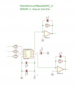
The gain of an IV stage is most appropriately expressed as a transimpedance. That is volts out per mA in. With 660R and 4mA input you'll get an output swing (peak to peak) of 2.64V. If you increase those fb resistors by a factor 10 the output swing would in theory go to 26.4V which in practice it can't because you don't have enough volts on the supply. So you'll get clipping (i.e. distortion). Somewhere in between 660R and 6.6k you'll find a happy medium - most headphones are playing plenty loud at 2VRMS so perhaps 1k5? That gives you 6V swing and easily handled on +5/-5V rails.
The gain of an IV stage is most appropriately expressed as a transimpedance. That is volts out per mA in. With 660R and 4mA input you'll get an output swing (peak to peak) of 2.64V. If you increase those fb resistors by a factor 10 the output swing would in theory go to 26.4V which in practice it can't because you don't have enough volts on the supply. So you'll get clipping (i.e. distortion). Somewhere in between 660R and 6.6k you'll find a happy medium - most headphones are playing plenty loud at 2VRMS so perhaps 1k5? That gives you 6V swing and easily handled on +5/-5V rails.
Understood 👌I plan then to try this out and report back here when the chips arrive. Lots of thanks again!
There's one further thing that I don't think we've talked about, and that is offset. Seeing as the output of the DAC chip is unipolar, the output of the opamps will be the same unless a circuit is included to offset the zero point. Without a level shifting circuit, the 6V swing cannot be accommodated on +5/-5V rails.
Thank you for pointing this out @Abrax. I will gladly get into it, although I'm not completely sure about what are you exactly referring to with 'offset'.
Here I share the general idea for powering both the DAC and the IV/HPA opamp. One amp of an AD712 is used to split the 12v rail into +/-6v, to feed the IV/Headphone opamp. The other AD712 amp is used as a linear 5v regulator using a zener, to feed the DAC.
The 12v power source (VCC1) are 3 x 4v lithium batteries in series. The 8v source for the DAC regulator (VCC2) is simply taken from the second battery in the series.
Please let me know what do you think about it, or did you want to discuss something else?
Is your schematic drawn as you intended? I ask because you said one half of the AD712 is a rail splitter but AD712-A has its +ve input connected to the V+ (positive power pin). I'd have guessed R217 & R227 were doing rail splitting.
I fear your scheme (even with the mid-rail opamp corrected) won't work because you have TDA1387 referenced to 'GND' which from the opamp's pov is V- - this forces the DAC's output compliance beyond its working range. AD8397's +ve input pin must be between GND and GND+3.5V for the DAC to function. There may also be a limitation imposed by the AD8397's common-mode input voltage range but the datasheet doesn't seem to offer any information on that.
I fear your scheme (even with the mid-rail opamp corrected) won't work because you have TDA1387 referenced to 'GND' which from the opamp's pov is V- - this forces the DAC's output compliance beyond its working range. AD8397's +ve input pin must be between GND and GND+3.5V for the DAC to function. There may also be a limitation imposed by the AD8397's common-mode input voltage range but the datasheet doesn't seem to offer any information on that.
I see what do you mean and think I start to understand. You are right with the rail splitter (AD712-A), I messed up with one connection VCC1 goes to the other corner of R227. :s
But also I see now why this is not gonna work. So to clear out things a little bit for myself (before drawing), the unipolar DAC will output a wave that can swing between 0 and 3.5v (DC output voltage compliance). Then we have to feed the inverting input of AD8397 from the midpoint of this wave, to comply with the bipolarity of the opamp. To do this I have to pull down the DAC output in -1.75v in theory... Correct? My intuition to do that is to put a pair of resistors of the same value before the inverting input of the opamp, as voltage divider. One resistor from signal to the opamp inverting input and the other to ground, this way the shift accommodates to the actual voltage at each instant. But this is just an intuition and a start, it is great to understand but wouldn't of course pretend to discover the wheel again.
But also I see now why this is not gonna work. So to clear out things a little bit for myself (before drawing), the unipolar DAC will output a wave that can swing between 0 and 3.5v (DC output voltage compliance). Then we have to feed the inverting input of AD8397 from the midpoint of this wave, to comply with the bipolarity of the opamp. To do this I have to pull down the DAC output in -1.75v in theory... Correct? My intuition to do that is to put a pair of resistors of the same value before the inverting input of the opamp, as voltage divider. One resistor from signal to the opamp inverting input and the other to ground, this way the shift accommodates to the actual voltage at each instant. But this is just an intuition and a start, it is great to understand but wouldn't of course pretend to discover the wheel again.
The DAC outputs a current and normally wants to see a fairly constant voltage on its output as the current swings from +1.08mA down to +0.08mA. The opamp by action of large gain and feedback keeps its two input terminals quite close together in voltage. So we just need to choose a voltage between 0 and 3.5V for the +ve pin and that'll set the DAC output (on the -ve input) at the same voltage no matter the current coming out.
It seems you're still thinking that the DAC's output is a voltage and its difficult to think in another mode - current.
It seems you're still thinking that the DAC's output is a voltage and its difficult to think in another mode - current.
Sorry, I tend to forget that the DAC outputs current :s I'm slowly getting there.
The voltage for the +ve has to be fixed? Should I for instance use a 3v zener (this is the lowest I have)? Or a voltage divider giving ~2.5v would be enough? I could place a pair of resistors dividing the 5v of the DAC power source confronting the +ve.
The voltage for the +ve has to be fixed? Should I for instance use a 3v zener (this is the lowest I have)? Or a voltage divider giving ~2.5v would be enough? I could place a pair of resistors dividing the 5v of the DAC power source confronting the +ve.
If the voltage at the +ve input varies it won't affect the DAC much but any variation on that pin will get passed on with a gain of 1 to your output (and hence your headphones). The challenge with this design is having the +ve pin at a voltage which suits both the DAC and the opamp. With a single supply arrangement I've solved that problem in one of two ways in various designs I've done.
1) Raise the DAC's GND pin a few volts (say 3V-4V) with a zener so that its output compliance range includes your mid-rail voltage.
2) Include 2 common-gate MOSFETs to cascode the DAC's outputs - effectively this allows a higher compliance voltage
There is also a 3rd way - reduce the total supply voltage below 8V and set the DAC's VDD to 5.5V, then the mid-rail voltage comes just within the 0 - 4V compliance range of the DAC at 5.5V supply.
Option 1) means to inject 3v-4v onto the ground of the DAC, while leaving the ve+ of the opamp directly to GND? I interpret this way the opamp while take GND as 3v-4v below the DAC's minimum. Am I right?
The 3rd way sounds intriguing to me, but my power supply will swing from 8v to 6v, as batteries discharge. Not sure it is applicable for my case.
The 3rd way sounds intriguing to me, but my power supply will swing from 8v to 6v, as batteries discharge. Not sure it is applicable for my case.
Option 1) means to inject 3v-4v onto the ground of the DAC, while leaving the ve+ of the opamp directly to GND?
No, if you did that then the opamp's +ve input would be below the DAC's GND potential and may damage it. Negative voltages are definitely out of the compliance range. The idea was to leave the +ve input at mid-rail (to get maximum swing out of the opamp's output) and move the DAC upwards in voltage. Say +ve input is at 6V as before but DAC's GND is at +3.6V using a zener between pin4 of the DAC and circuit GND. Then the DAC output compliance range would be from +3.6V to +7.1V and 6V fits neatly within that window with some wiggle room.
I interpret this way the opamp while take GND as 3v-4v below the DAC's minimum. Am I right?
Here I can't quite get your question.
The 3rd way sounds intriguing to me, but my power supply will swing from 8v to 6v, as batteries discharge. Not sure it is applicable for my case.
One solution to this is include a regulator to give 8V stable output then use 3 LiIon batteries to feed that.
 Moved to Digital Line Level
Thanks for your patience @abraxalito. After thinking about it and trying to find a simple solution, maybe the following circuit will work. It lifts up the ground of the DAC in 3v using a zener and the first LiIon in the series. 3v is the cutoff voltage of the battery so I prefer it to a higher value. The DAC's VCC is taken from the second and third batteries, regulated at 5.1v by a zener. I removed the opamp linear regulator because maybe it was not necessary, since the overall consumption of 4x TDA1387 must be around 22mA max., well below the zener's max. current. Although I'm not sure if they will introduce perceivable noise.
GND is LiIon1(-).
Looking forward to hear any comments from you.
GND is LiIon1(-).
Looking forward to hear any comments from you.
Attachments

Do you know the 4V compliance range of the DAC at 5.5v by experience, or any other source? I don't seem to find that in the datasheet, where 3.5v max. is stated (p.8). But I like you 3rd way of going down to a 4+/- rail, it allows a fixed voltage for the AD8397 therefore headphones won't decrease gain as batteries drain. I'm afraid now that this is a problem in the diagram I just shared.There is also a 3rd way - reduce the total supply voltage below 8V and set the DAC's VDD to 5.5V, then the mid-rail voltage comes just within the 0 - 4V compliance range of the DAC at 5.5V supply.
I can't quite understand the reason for a connection to intermediate points within your LiIon stack. Seems to me that'll lead to a heap of pain as the cells discharge at different rates.
You're right, a 3V zener will be fine at 22mA - you can delete R232 (replace with wire) and the connection to the internal node of the LiIon stack. To feed the DAC+zener in series you could introduce a current source set to 27mA - 22mA for the DACs with 5mA for the 5V1 zener. A current source will do better than a resistor as the LiIon voltage varies over its discharge. The opamp might not need a regulated supply but I'd replace R217 with a zener to keep the voltage at the DAC output constant against LiIon voltage variation.
Yes I know the 4V max compliance by experience when the DAC's fed with 5.5V, its not in the datasheet which limits itself to parameters at the typical 5V supply.
A current source will do better than a resistor as the LiIon voltage varies over its discharge. The opamp might not need a regulated supply but I'd replace R217 with a zener to keep the voltage at the DAC output constant against LiIon voltage variation.
What do you mean here by 'current source'? A different type of circuit to limit current instead of voltage? Sounds useful.
Do you think I can get rid of the opamp feeding the opamp, using a simple resistor divider (with caps) and overall voltage set at 8v? The main reason is that the opamp takes space and is current limited (so I guess I would need two half opamps or a pair of transistors after it to feed the 45mA @ 2.9vRMS drawn by the headphones).
In the following diagram I'm trying to get rid of the 'heap of pain', with no connections between batteries–which was based on my ignorance on how to properly regulate voltage noiselessly and wish for transparency, I'm recently getting into zener regulators. It is mainly based on your own idea of a 'third way':
- Home
- Source & Line
- Digital Line Level
- Building a portable I2S 4x TDA1387 DAC