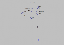
Current source schematic is attached. The terminal marked 'Out' goes to the cathode of D33, taking the place of R236. (D34 by the way is upside down).
Yes I think its a good simplification to delete the opamp. You can also delete C74.
Now we've gotten the DAC with appropriate output compliance voltages the last step is compensating for the offset. 1k8 resistors between both DAC outputs and GND should do the trick.
Yes I think its a good simplification to delete the opamp. You can also delete C74.
Now we've gotten the DAC with appropriate output compliance voltages the last step is compensating for the offset. 1k8 resistors between both DAC outputs and GND should do the trick.
Attachments
Thanks a lot for the schematic. Could I use a pair of BC559A as transistors for the current source?
https://www.onsemi.com/pdf/datasheet/bc559-d.pdf
If yes, resistor values would be the same?
I'll add the current source and your comments to the drawing 👍👍, but I'm slightly wondering what the actual advantage of a current source in this case would be. In theory the 5.6v zener-resistor voltage that feeds the DAC shouldn't be affected by battery drain, since it's source is a 8.2v zener regulated by a stable source (as itself is powered by min. 9v).
I wasn't intending you feed the current source from the 8.2V zener, rather directly from the LiIon stack. That's why I wrote 'VCC' on its power supply. I will check to see if BC559A are suitable and get back to you on that question.
I think the 8.2V zener scheme is problematic as shunt regulators (zener regulators are shunt type) always need to be biassed above the maximum current draw expected by the circuit they're powering. That circuit in your case is a classAB amplifier which draws a variable current depending on the music. If the headphones are 32ohm and driven by a max 2.8V signal that results in a peak current of 88mA per channel so 176mA totally. It will be a real waste of power to bias a zener at 180mA, not to mention a single 8.2V zener won't be able to sustain the power dissipation.
I think the 8.2V zener scheme is problematic as shunt regulators (zener regulators are shunt type) always need to be biassed above the maximum current draw expected by the circuit they're powering. That circuit in your case is a classAB amplifier which draws a variable current depending on the music. If the headphones are 32ohm and driven by a max 2.8V signal that results in a peak current of 88mA per channel so 176mA totally. It will be a real waste of power to bias a zener at 180mA, not to mention a single 8.2V zener won't be able to sustain the power dissipation.
I was realising today the situation with using different headphones, while trying to bias the 8.2v zener. Also, I see now that biasing the 5.6v zener will be also wasteful as voltage runs down, so the current source is more than welcome!
What would you recommend to power the opamp then, if not the shunt regulator? A linear regulator I guess but I was also trying to avoid it, if possible.
Should I maybe then go back a bit to the previous design maybe? Where the DAC GND is raised in 3V by a zener (directly from VCC), DAC VDD fed by a 5.6v current source (as per your scheme) and run then the divider/opamp directly from the 12v VCC.
Biasing the 5.6V zener is only wasteful to a small degree as the maximum current is close to the typical operating current.
You could try feeding the opamp directly from the LiIon stack and see how that works out. If that turns out no good then yes a linear regulator is the next best solution.
BC559s should be fine for the CCS. The max dissipation is just under 200mW at the highest battery voltage (12.6V).
You could try feeding the opamp directly from the LiIon stack and see how that works out. If that turns out no good then yes a linear regulator is the next best solution.
BC559s should be fine for the CCS. The max dissipation is just under 200mW at the highest battery voltage (12.6V).
Hi Abrax. Do you think the following diagram will work? The zener for the CCS is 8.2v, so with the addition of the 3v zener at the DAC's ground we meet 5.2v VDD. Since the opamp GND is -6v max. /-4.5min., the DAC's output voltage should be set between 3-1.5v.
I don't fully understand how your CCS circuit works internally, but I think I was able to tweak the resistor values using a simulator to provide 25mA @ 5.2v at the load. 20mA for the DAC, 5mA for the 3v zener. Extra 5mA for the 8.2v zener are also considered.
If you see any problems to it, or any component that could be reduced in size (ie. the 220u cap. for the resistor divider), please let me know.
Attachments
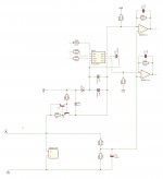
Now you've arranged the DAC's output voltage to track along with the discharge of the LiIons, the 1k8 resistors no longer act as current sources because the voltage across them is changing. I'm not sure whether this will turn out to be an issue in practice - your HPs will be AC coupled so it won't concern them.
Your version of the current source has 18R to determine the current, I'm getting ~33mA output current (0.6V/18) and wonder why you'd want it so high? Your DACs are taking ~22mA and the 8.2V zener needs a few (2-5) mA to regulate. The 3V zener's current doesn't enter the equation - that'll be whatever the DACs are drawing.
Apart from these minor points, everything else is looking good now. Remember the GND for the I2S input needs to be DAC GND (TDA1387 pin4) not battery GND.
When you say GND for I2S input do you mean the source of the digital signal? If that's the case I would be in real trouble, because the source is an ARM that produces a lot of noise and is therefore powered by its own single LiIon, so no way I can raise its ground voltage in 3v as well. Unless I would integrate the MC to the 12v stack and isolate it somehow. Also the clocks are generated by it.
I can go back to the values you suggested for the CSS, I thought the 3v zener needed it's own extra current :s
I can go back to the values you suggested for the CSS, I thought the 3v zener needed it's own extra current :s
The source's GND needs to be connected to the DAC chip's GND (pin4). I can't see why there would be any problem when both are powered by their own LiIon cells. You're not raising the source's GND voltage, you're raising the DAC's GND relative to its own power source (which is isolated).
I understand. Relief. Got confused because I have at least an ADC and a 12v preamp behind the DAC and thought for a moment all that had to be lifted up on their own as well. Very important tip anyways. That ADC GND will be on the 3v by default, since I'm planning to use the same 5v of the DAC for it. Therefore–and by the way, I'll have to rise the CCS in about 30mA or whatever that ADC will consume...
How do you calculate the output current of the CCS? I know for instance that 0.6v/18 is 33mA by ohm's law. But where do you take the 0.6v from? And what's the relation with the 3.3k resistor? I tried to find this topology of CCS online but couldn't find any alike, very effective for the few parts on it. I cannot expect a full explanation here anyways of course.
How do you calculate the output current of the CCS? I know for instance that 0.6v/18 is 33mA by ohm's law. But where do you take the 0.6v from? And what's the relation with the 3.3k resistor? I tried to find this topology of CCS online but couldn't find any alike, very effective for the few parts on it. I cannot expect a full explanation here anyways of course.
The 0.6V is a number arising from the properties of a silicon diode, or here a base-emitter junction in a transistor (T4 in your most recent schematic). When T4 conducts there will be about 0.6V across the resistor between its base and emitter. Where is a 3.3k resistor appearing from?
On the CCS, here is a very useful resource : https://sound-au.com/ism.htm#p5 Note he's using 0.65V whereas I use 0.6V.
On the CCS, here is a very useful resource : https://sound-au.com/ism.htm#p5 Note he's using 0.65V whereas I use 0.6V.
Good read. Thank you! I meant the function or way to calculate the adequate value of the resistor going from Q2's base to ground (R3 in Elliot's diagram B). You suggested me a value of 3.3k for this resistor.
Oh that resistor is normally calculated to supply a bias current of 5-10% of the CCS output current. If we go for 5% then with the CCS putting out ~30mA it should carry a current of 30/20 or 1.5mA worst case (lowest supply voltage). Which results in a value of 4k7.
Perfect. Now I can design my own CCS 🙂
The diagram above (V6) is then definitely to try, but I'm still hesitating about the effects of battery discharge on the opamp, now that I got more into it and different possibilities
In the previous design (v5), where the 12v stack was reduced to 8.2v and from there a stable 4+/- rail was produced, the problem was excessive power consumption by the zener resistor (particularly when batteries were full, if the zener was calculated at the minimum voltage). Would a linear regulator build with an opamp and a zener voltage reference solve that problem? I'm supposing that, if a zener would only provide a vf on the non-inverting input, power consumption should be proportional to the variable load (ie. different headphones). But maybe the intrinsic power dissipation of the opamp, stepping down from 12v to 8v itself will also be significant? Just wondering to give a chance to the other design as well, I'm realising that that would be a safer design and possibly I'll have a spare opamp to use.
Any idea on how could I implement a volume control to this design, @abraxalito?
I guess a pot directly on the DAC's output would be disastrous, since that's a current output? I also thought of a 1k in place of the feedback resistors of the opamp :s. A pot on the opamp's output would introduce too much impedance and affect high frecuencies I suppose (volume pots never go at a headphones amp output).
The alternative is to attenuate the I2S source signal digitally with a pot, but analog would be of course much better.
Adding on a volume control is always a bit tricky. If you have a low enough value of stereo pot (say 1kohm) you could just wire that in parallel with R234 and R240 in your latest schematic. That would be the easiest solution but 1k stereo pots aren't that easy to find.
The next easiest solution is to add another stage (second dual opamp) and put the volume control between first and second opamp. The second stage opamp would be configured as buffer (unity gain). Then the volume control could be 5k or 10k, fairly easy to find values.
Another possibility is to vary the pin7 reference voltage downwards from its 0.83V typical value - this can be done with a pot between pin7 and pin4 but it exposes the pot to DC which they don't like normally. The advantage of this method is you only need a single gang pot as both channels follow the Vref pin voltage together.
Digital volume control is another solution but that would need some coding skills I would guess, I don't know of a stand-alone IC which implements volume control on an I2S stream. You can't use a pot for digital attenuation but you can use a pot to indicate a volume level to an MCU which then does the volume control. The digital volume software needs to perform multiplication and dither followed by truncation to 16bits.
Thanks a lot, I'll try all these options and comment after. Adding another opamp would take too much space, but I'll try adding a 1k in parallel to a 10k pot so it behaves like a 1k and see the linearity I get with that in parallel to R234/R240. Lowering the voltage of pin7 sounds genius and want to hear it at work.
BTW, a digital volume control is easy with a Teensy, since they have an online tool with modules and one of them ready to implement gain control ('amp' it's called). It only needs to be assigned to a rotary knob. But I'm a bit skeptical of distortions, digital noise and battery drain that it might introduce. It all needs to be tried out 🙂
BTW, a digital volume control is easy with a Teensy, since they have an online tool with modules and one of them ready to implement gain control ('amp' it's called). It only needs to be assigned to a rotary knob. But I'm a bit skeptical of distortions, digital noise and battery drain that it might introduce. It all needs to be tried out 🙂
Adding 1k in parallel with a 10k pot won't make it behave like a 1k pot. The main issue is the resistance change vs rotation characteristic, added to that the mutual tracking of the L/R channels. Certainly have a try just sticking your 10k pot in parallel with the 620R already in-circuit and see what happens. You'll find that over the bulk of the travel you hardly notice any change in volume then all of a sudden it'll go quiet right at the end.
Teensy does sound like an interesting way to do digital volume. The only downer for Teensy that I see is its proprietary hardware rather than open. In terms of battery drain Teensy uses ARM so it'll not be a huge drain so long as you use a buck reg to power it. The earlier Teensies were (I think) using Cortex M4 which consumes about as much power as a single TDA1387. The latest one has a red-hot M7 at 600MHz so is more hungry but you can always scale down the clock rate to save power.
Teensy does sound like an interesting way to do digital volume. The only downer for Teensy that I see is its proprietary hardware rather than open. In terms of battery drain Teensy uses ARM so it'll not be a huge drain so long as you use a buck reg to power it. The earlier Teensies were (I think) using Cortex M4 which consumes about as much power as a single TDA1387. The latest one has a red-hot M7 at 600MHz so is more hungry but you can always scale down the clock rate to save power.
@abraxalito
Is there any easy way to get 0 VDC output with passive IV in order to eliminate coupling caps?
Is there any easy way to get 0 VDC output with passive IV in order to eliminate coupling caps?
I can't think of one, no and I've given it some thought over a long timeframe.
Alternatives are - a servo, but that always uses a cap though it can be a smaller value. A digital servo using an MCU can work without a cap though.
Alternatives are - a servo, but that always uses a cap though it can be a smaller value. A digital servo using an MCU can work without a cap though.
- Home
- Source & Line
- Digital Line Level
- Building a portable I2S 4x TDA1387 DAC