You don't need to have pin5 at 5.5V when you use a cascode. You have more flexibility with power supply voltage because the voltage variation on the source of the MOSFET (connected to the DAC's output) becomes much less than without the MOSFET. Without the FETs we looked for ways to increase the output swing and increasing the supply voltage is the easiest way to achieve that.
With the cascode the voltage swing is determined by the I/V resistor and the number of paralleled chips. Say you used 6 chips and went for 2k I/V then the swing would be 6*2 = 12V for 5V on pin5.
I need to look up the 1.8k resistor as my memory fails me on that. Ah yes, the 1k8 was to compensate for the current out of the DAC being uni-directional rather than bipolar. The way you have your schematic at present the DACs always source current so the opamp always has to sink it. To get the opamp output to the middle of its supply rails you need to 'bleed away' some DAC current so that at digital zero the opamp isn't sinking any current.
Last edited:
That's very clear.
1. Do you have any comments on the opamp's output cap? I used a large value of 330u, thinking that with 63ohm impedance HPs it would high pass at 7Hz. Then added a 100K resistor to GND between cap and GND, so DC damps through it also, but not sure really if that makes sense.
2. Also, in the schematic above I use a TL431 as vref. Should I add an extra capacitor between the TL431's ref and its cathode? I've read that it is necessary to improve the regulator's output impedance, but not sure if that's the case here.
3. If the cascode's swing is 6Vp, like in your example, my HPs will sound too loud and consume too much current. Say I need a swing of 2.5Vp only, but that's too low for the opamp's input from ground, which will probably clip. Now the opamp is nicely seeing 2.5V at 5.5V midrail, because of the 'ground lift'. But without the lift and according to your example, the opamp will see 6V from ground and be super loud/consuming. Maybe I'm just misinterpreting here, but I'm just afraid that the effort of designing with Mosfets will result in my case in even more battery drain.
1. Seems fine. I usually go for bigger than needed output caps.
2. Seeing as your Vref is 2.5V no cap has any real effect (the 3k01 resistor is also redundant).
3. In your case with opamp I/V the function of the cascode is really as a level shifter - there isn't going to be much swing at the opamp input as that's a 'virtual GND'. So because there's no output swing, that advantage of the cascode is irrelevant. With the cascode FETs the opamp can run happily on a higher voltage and still have its inputs at mid-rail. Conversely the DACs could be run at lower voltage to save some power. Without the cascodes the opamp's supply voltage is limited to about 7.5V (so that mid-rail falls within the DAC's compliance range).
2. What do you mean 3k01 for the TL431 is redundant? That it could be much higher, or that no resistor is needed there at all :s?
Now to the matter. A level shifter for the DAC's output is exactly what I need! Rather than shifting the entire circuit behind.
But the challenge of understanding MOSFETs and the cascode configuration is beyond my time limits at the moment, I would be pleased enough with a working circuit to test and prototype. Is the schematic attached going in the right direction? Notice that I raised the TL431 to 5.5V and all is now grounded to 0V.
Shame on me for not understanding what I'm drawing here and infinite gratitude to your support so far.
Attachments

Dear Abraxalito,
Could you please guide me to lift the output voltage over the compliance using mosfets? I've got today a few 2N7002 I've ordered before to experiment but I'm pretty much clueless what to do with them. 😕
In the Dorati you seem to use only one Mosfet per channel, biased on the gate at 3.2V with a series 120R. This followed by a current source and an LC filter. This seems to me is not a cascode configuration and forms an I/V filter only (no lift).
In another post you share a diagram for headphone buffer which uses 2 Mosfets. This seems closer. You mention that's a high power version (probably too much for my low impedance headphones) of another you have in your blog, but surfing your blog I can't find it.
2. What do you mean 3k01 for the TL431 is redundant? That it could be much higher, or that no resistor is needed there at all :s?
When I looked at your schematic you had the TL431 set up for 2.5V. In this configuration it just needs a short from cathode to adjust. (I think you might have had a very low value R there like 1 or 2R). So 'no resistor is needed there at all' is my meaning.
But the challenge of understanding MOSFETs and the cascode configuration is beyond my time limits at the moment, I would be pleased enough with a working circuit to test and prototype. Is the schematic attached going in the right direction? Notice that I raised the TL431 to 5.5V and all is now grounded to 0V.
The schematic is only for one channel but you have two MOSFETs there. Only one is needed per channel - connect the FET in the same way you will have seen when looking at my Dorati schematic. Source to DAC, drain to opamp and gate to a VREF which depends on which FET you choose.
In the Dorati you seem to use only one Mosfet per channel, biased on the gate at 3.2V with a series 120R.
Yes - the 120R is there to stop the FET oscillating, its called a 'gate stopper resistor'. Its value isn't too critical. Having about 3V on the gate sets the source to be about 1.2V, depending on the FET.
This followed by a current source and an LC filter. This seems to me is not a cascode configuration and forms an I/V filter only (no lift).
Actually there are two current sources needed (as I think I've mentioned before) - one on drain (to +ve supply) and one on source (to 0V). It does implement a lift function because the DAC's output (FET source) is only around 1V and the opamp input (FET drain) is at mid-rail, which on Dorati is set to just below 5V.
In another post you share a diagram for headphone buffer which uses 2 Mosfets. This seems closer. You mention that's a high power version (probably too much for my low impedance headphones) of another you have in your blog, but surfing your blog I can't find it.
In a headphone buffer it seems I wouldn't be using a cascode, maybe it was a source follower? I'm not sure which diagram you're referring to so I can only make a wild guess.
Meantime I've been experimenting with a class AB (two transistors and 2 diodes) as output stage. It sounds impressively good compared to opamps and not that more consuming. Problem is again max. input voltage is too low for a simple voltage follower, because of the DAC's output limitation. So I'm experimenting now with a three transistor AB, with an input driver NPN to increase voltage. Seems getting somewhere in simulations.
If a MOSFET is used instead of an NPN as driver for a class AB–at the output of the DAC as we have spoken before, would I still need a current source at drain like in the Dorati? AND/OR at source?
Very glad to hear from you again.
If a MOSFET is used instead of an NPN as driver for a class AB–at the output of the DAC as we have spoken before, would I still need a current source at drain like in the Dorati? AND/OR at source?
Very glad to hear from you again.
Meantime I've been experimenting with a class AB (two transistors and 2 diodes) as output stage. It sounds impressively good compared to opamps and not that more consuming.
My experience too - using discrete circuits often sounds impressive compared to using opamps.
Problem is again max. input voltage is too low for a simple voltage follower, because of the DAC's output limitation.
That's the reason for the MOSFET cascode. You don't need any further voltage amplification, just choose a high enough I/V resistor.
So I'm experimenting now with a three transistor AB, with an input driver NPN to increase voltage. Seems getting somewhere in simulations.
Using a voltage gain stage will always lose out, noise-wise, to a larger value I/V resistor.
If a MOSFET is used instead of an NPN as driver for a class AB–at the output of the DAC as we have spoken before, would I still need a current source at drain like in the Dorati? AND/OR at source?
In your description there doesn't seem to be enough detail for me to know the configuration of the MOSFET.
In your description there doesn't seem to be enough detail for me to know the configuration of the MOSFET.
I meant to use a MOSFET in a cascoded configuration as you have suggested, to be able to use a higher I/V resistor and avoid having to amplify the DAC's output with a common-emitter / driver stage.
The current sources at drain and source, which I see now clearly in the Dorati, unfortunately take up too much board space. I wonder if TO-92 current sources like the LM334 could be also used instead. But the idea is fantastic! The currents they draw depends on the type of MOSFET? Or (also) on the DAC's available output current/number of chips used?
And where would the I/V resistor go? Right after the drain I suppose? I can't seem to find it in the Dorati's diagram.
The current sources at drain and source, which I see now clearly in the Dorati, unfortunately take up too much board space.
I guess you are using through-hole parts (you mentioned TO-92). In SMD a current source occupies about 5*5mm. You can save space on the lower (to 0V) current source at the loss of some performance. You can change it to a resistor - reason being the MOSFET source voltage does not vary very much (perhaps 0.2V peak to peak) so a resistor can be a close enough approximation to a CCS (abbreviation for constant current source). On the drain side the voltage variation is very large so a resistor can't simplify things.
I wonder if TO-92 current sources like the LM334 could be also used instead. But the idea is fantastic! The currents they draw depends on the type of MOSFET? Or (also) on the DAC's available output current/number of chips used?
LM334 will work (I haven't tried it) though it might turn out a bit noisy. Yes the CCSs depend on the number of chips. The lower CCS needs to be set a couple of mA higher than the maximum current out of the DAC chips. So for six chips (6mA) you'll want 8 or 9mA. The extra current keeps the MOSFET conducting even at digital full-scale.
And where would the I/V resistor go? Right after the drain I suppose? I can't seem to find it in the Dorati's diagram.
Yes, it goes from the drain to your mid-rail voltage (on Dorati: Vref). R9 and R36 are I/V resistors on Dorati.
You have encouraged me. I will try this with a resistor on the source instead, to make things easier for me and knowing it's a bit of a bad practice.
What about the CCS at drain? Should it provide the same current than the resistor/CCS at the source? I ask because in the Dorati I see different values for both CCS–the current source at MOSFET source looks more like sink to me.
You guess right. My resistors are also 4 times the size they should be 😀 This is one my first prototypes though, I might come down at some point to printed boards and all SMD scale.I guess you are using through-hole parts
The lower CCS needs to be set a couple of mA higher than the maximum current out of the DAC chips
What about the CCS at drain? Should it provide the same current than the resistor/CCS at the source? I ask because in the Dorati I see different values for both CCS–the current source at MOSFET source looks more like sink to me.
The CCS at drain needs to draw enough current so that at digital zero there is no current through the I/V resistor.
Assume we have 3mA extra on the lower CCS, making it 9mA. At digital zero the DACs put out 580uA, so with 6 of them there's 3.48mA. What's left is 9-3.48mA = 5.52mA. So that's what's needed in the top CCS.
Assume we have 3mA extra on the lower CCS, making it 9mA. At digital zero the DACs put out 580uA, so with 6 of them there's 3.48mA. What's left is 9-3.48mA = 5.52mA. So that's what's needed in the top CCS.
 I don't know much and can't imagine how many people know more than me, but you are genius and bless you for all the sharing. I'm good to go now, until then.
Abraxalito, just a question.
Isn't there a way to inject current into the output of the DAC, using a current source and a sink for example, so it remains an I-out to drive headphones directly but at a higher current (without dealing with voltages at all)? The problem with pilling up tens of chips is that efficiency comes down to less than 20% (1mA out per 5.5mA consumed). Quite hard for batteries. But nothing I've heard so far compares to the transparency of going directly with cans to the output. I've had few times the impression, or illusion, that there might a way to bring in extra current externally, without dealing with I/V resistor, caps, filters and voltage in general. If that's just called an amplifier and this sounds like no sense, I can easily bring this idea down to rest.
Isn't there a way to inject current into the output of the DAC, using a current source and a sink for example, so it remains an I-out to drive headphones directly but at a higher current (without dealing with voltages at all)? The problem with pilling up tens of chips is that efficiency comes down to less than 20% (1mA out per 5.5mA consumed). Quite hard for batteries. But nothing I've heard so far compares to the transparency of going directly with cans to the output. I've had few times the impression, or illusion, that there might a way to bring in extra current externally, without dealing with I/V resistor, caps, filters and voltage in general. If that's just called an amplifier and this sounds like no sense, I can easily bring this idea down to rest.
State of the art of this DAC.
At the output a class AB amplifier intended for headphones. Stacking 24x DACs took too much battery power, so the idea here is that the amplifier injects the extra current needed. Voltage swing is supposed to be the maximum TDA1387 can provide.
A transistor-based ground lift is supposed to be more quiet than a series zener. Reference voltage is taken directly from the first Li-Ion of a 3x series, 3V/9V the absolute minimum. The NPN between 3V and lift PNP compensates for the voltage drop, so ground lift remains at the value of the first battery. R133 is there to relief the load on the lift transistor, in case more devices operate in parallel to the DAC.
The resistor to ground of the AB class amplifier (R126) operates as I/V resistor and 1st order LPF with inductor L51. The filter is basic because a digital filter would be used at the I2S source and I had no more space/knowledge to design a better one. I'm not sure if the inductor could be unshielded, how crucial that is being an inch away from the MCU all well routed and grounded on a plane. Shielded inductors are bigger and difficult to obtain.
Any comments on this? @abraxalito ? In simulation it works, breadboarding I've had grounding/noise problems I'm planing to print a PCB.
Regards,
Domingo
Ground lift looks fine, the BD559/BC559 current source looks wrong somehow - base of BC559 should go to the 18R and its emitter to 9V. Its collector goes to base of BD559 and R119. Then there's the issue of insufficient headroom - with 3V and 5.6V you get to 8.6V and the CCS needs more voltage than 0.4V across it to operate - typically I find 0.8V is the minimum. But perhaps your 9V is actually higher in practice.
Looking across to the right, assuming TS5 collector is supposed to go to 9V then you'll have an effective I/V resistor of 1.35k so a total swing of 1.35V which might depend on the load impedance (and the current gain of TS5 & 6). I can't quite see the function of the 10mH.
For more mA output per mA of supply current, the comms DACs (e.g. AD9764) are very hard to beat. But to use one of those you'll need your CPU to interface it as they're parallel input.
Thanks for the reply @abraxalito, always a pleasure to hear from you again. I apologise for the mistakes on the drawing, I made it in a run puzzled by the output stage. Corrections on the left side are exactly as you say.Ground lift looks fine, the BD559/BC559 current source looks wrong somehow - base of BC559 should go to the 18R and its emitter to 9V. Its collector goes to base of BD559 and R119. Then there's the issue of insufficient headroom - with 3V and 5.6V you get to 8.6V and the CCS needs more voltage than 0.4V across it to operate - typically I find 0.8V is the minimum. But perhaps your 9V is actually higher in practice.
Looking across to the right, assuming TS5 collector is supposed to go to 9V then you'll have an effective I/V resistor of 1.35k so a total swing of 1.35V which might depend on the load impedance (and the current gain of TS5 & 6). I can't quite see the function of the 10mH.
For more mA output per mA of supply current, the comms DACs (e.g. AD9764) are very hard to beat. But to use one of those you'll need your CPU to interface it as they're parallel input.
Do you think it is a good idea to use a ground lift in this case? My assumption is that it saves me parts on the output stage (the I/V resistor and decoupling capacitor) which should increase sound quality.
The intended function of the inductor was to form an LR filter with R126 (2.7k). I see now that it doesn't work I guess because there's no yet voltage. Still thinking how to a include a 1st order LPF for safety. I have a few old chips AK4384 I might try instead of the TDA1387 as well on the same board prototype/output stage, it might sound good with a simple class AB, but I'm a bit afraid of printing a prototype without any analog LPF.
TDA1387 outputs around 1mA per chip... This is per channel or in total? This is a question that came back to me since a while.
And is the resistance that the DAC sees somehow affected by the fact that DAC and I/V resistor are grounded, on this diagram, at different voltages?
Whether its good to use the ground lift is really about whether it achieves your purpose. I've used it on a few DAC designs to position the output range of the DAC where I want it to be. Its easier when the DAC part is powered separately from the source because then you won't have to worry about level shifting the inputs.
Maybe the inductor works as a filter, I haven't looked closely but it'll certainly increase the output compliance of the DAC which is an undesirable side-effect. There's no damping on the L when driven by a current source. You do need to take account of not just one resistor when working out the load (the R part) the L is seeing. Hence 1.35k, not 2.7k. This is assuming the diode dynamic impedance is negligible compared to the resistors.
1mA is per channel, so 2ma totally L and R together. You can increase that with an R between pin7 and pin5. I use 100k to give me 1.5mA but there's no free lunch, the supply current goes up in proportion.
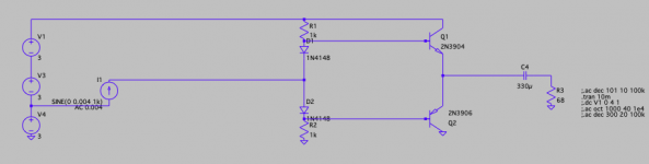
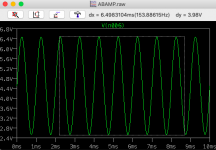
Is it maybe the case that I'm missing something in the simulation? Only for testing purposes (the example falling below the DAC's compliance voltage): a voltage divider of 1k is producing 4Vpp on a 4mA source (4x DAC) in the simulation. This is to expect from a single single I/V resistor to GND. Two 1k in parallel should give 500ohm therefore 2Vpp.You do need to take account of not just one resistor when working out the load (the R part) the L is seeing. Hence 1.35k, not 2.7k. This is assuming the diode dynamic impedance is negligible compared to the resistors.
If that is the case, would you know how to simulate it correctly?
Attachments
Last edited:
- Home
- Source & Line
- Digital Line Level
- Building a portable I2S 4x TDA1387 DAC