The Idss of the JFET's is a bit high, around 8.5mA.
I'm getting 0.062V on R20-R24, so higher than 0.01-0.04 target but generally should be OK I think.
WHoa!!! Did you buy the JFETs from the DIYAUDIO store? If not, you may have bogus K170's Idss of "B" class K170's is ~6 to 10mA
I bought from bdent.com and they look legit based on the markings (the font, physical dimensions etc).
Correct me if I'm wrong but ~6 < 8.5mA < 10mA .. what am I missing ?
Correct me if I'm wrong but ~6 < 8.5mA < 10mA .. what am I missing ?
WHoa!!! Did you buy the JFETs from the DIYAUDIO store? If not, you may have bogus K170's Idss of "B" class K170's is ~6 to 10mA
I have 2 Pearl boards, and 2 Mini Pearl boards. 2SK170B in the Pearl and LSK389B in the Mini -- each JFET draws 6.6 to 7.0mA. If the Idss for your JFETs is 8.5mA, you're gonna pull 34mA across R9 so the voltage on the emitter of Q3 will be lower. I wouldn't be alarmed at all with the higher Idss.
Some bogus JFETs are switching devices with Idss of ~50mA
Thanks for the info Jack.
Each JFET draws 6.2mA (measuring R21-R24)
I'm not concerned at this point at the higher Idss, but rather Q3 voltages.
Ve=7.64V, Vb=8.38V but Vc=7.78V ... whereas it seems it Vc should be higher than Vb?
Each JFET draws 6.2mA (measuring R21-R24)
I'm not concerned at this point at the higher Idss, but rather Q3 voltages.
Ve=7.64V, Vb=8.38V but Vc=7.78V ... whereas it seems it Vc should be higher than Vb?
The higher bias of the Jfets will increase the voltage across R9 (499R) and less voltage on Q3's collector to emitter and I would think you would want at least a volt or so collector to emitter on Q3.
Solutions could be:
1) Different Jfet Idss. Which is what the circuit was designed for
2) Lower R9, thus reducing the gain.
3) Lower the voltage on Q3's emitter by changing R8 and R10 ratio, thus
lowering the voltage on the Jfets drains.
How much any of these changes would effect the overall circuit performance I don't know? You are close, so some minor changes to a couple of the values would get you there.
Thanks BDP.
The circuit was designed for BL which is ~6-12mA base on the datasheet.
Somewhere in this thread, the recommendation is for 5-6mA JFET's, but that seems fairly hard to get. I purchased 62 JFET's and measured all of them, the vast majority was in 9mA-11mA. I barely managed to find 2 quads in the ~8.5mA range.
So (1) is out of question for me.
One additional option that some folks suggested was increased R21-R24 to 20R from 10R.
I tried earlier to put a 27.5K resistor (just something I had) in parallel to R10 bringing it down to 7.2K. It made a little difference, Vc was still below Vb.
Is there a preferred option out of these?
Options?
You could raise the source resistors, thus lowering the Jfets current?
You could remove one of the Jfets?
I think the best solution is to tweak a couple of resistor values that way you are not to far from the intended design.
You could raise the voltage on the emitter of Q1 by a volt and at the same time lower the voltage on the emitter of Q3?
What is the voltage on Q1 emitter?
With stock values emitter of Q3 should be about 9.5 volts. You measured Ve=7.64V? Was this with 27k in parallel with R 10?
What is the voltage on Q1 emitter?
With stock values emitter of Q3 should be about 9.5 volts. You measured Ve=7.64V? Was this with 27k in parallel with R 10?
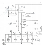
Attached are my measurements. This is with all stock values, i.e 10K for R10.
Stock pearl -- here are my voltages:
Jack, it looks like our voltages are very similar, in particular with regards to Q3.
There isn't any issue with my build then?
If so, what is all the discussion on this thread around Vc needing to be higher than Vb ?
Attachments
Try this,
Raising Q1 emitter voltage to 21 volts and lowering the Q3 emitter voltage a couple of volts would get you there.
To raise Q1 emitter voltage parallel a 3K resistor with R5, 1.5//3K.
Check Q1 emitter voltage.
To lower Q3 emitter voltage parallel a 20K resistor with R10, 10k//20k
This should provide about 1 volt on Q3 collector to emitter and reverse bias the base to collector junction.
All this is because the Jfets Idss, Vgss, is to high for the design. Jfets Vgs of up to .05 volts would keep Q3 biased correctly.
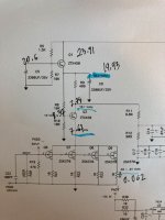
I was only able to find 3.3K and 27.5K .. good enough for the experiment.
3.3K in parallel to R5 resulted in 20.8V at Q1 emitter.
With 27.5K in parallel, result is:
Vc = 8.6V
Vb = 8.2V
Vc = 7.5V
Looking better....
So if I want to permanently change resistors, looks like I need something like
R5 = 1K
R10 = 6.5K ?
3.3K in parallel to R5 resulted in 20.8V at Q1 emitter.
With 27.5K in parallel, result is:
Vc = 8.6V
Vb = 8.2V
Vc = 7.5V
Looking better....
So if I want to permanently change resistors, looks like I need something like
R5 = 1K
R10 = 6.5K ?
Almost there. Do you have two 10k resistors to put in series to try?
You could also try a 10k // with R10, this would be about 6.3 volts on the drains of the Jfets (Q3 emitter), with this your losing another 1.5 volts and getting further away from the intended design, but it will work.
You could also try a 10k // with R10, this would be about 6.3 volts on the drains of the Jfets (Q3 emitter), with this your losing another 1.5 volts and getting further away from the intended design, but it will work.
OK got two 10k resistors...
Results are now
Vc=8.55V
Vb=7.8V
Ve=7.1V
So not much different than the 27.5K, just lower voltages overall.
Results are now
Vc=8.55V
Vb=7.8V
Ve=7.1V
So not much different than the 27.5K, just lower voltages overall.
So if I want to permanently change resistors, looks like I need something like
R5 = 1K
R10 = 6.5K ?
Closest standard value 6.49K, 6.65K, 6.81K
OK got two 10k resistors...
Results are now
Vc=8.55V
Vb=7.8V
Ve=7.1V
So not much different than the 27.5K, just lower voltages overall.
But the Q3 Vbc is now reversed biased and your Vce is a little more than 1 volt.
Looking good🙂
Thanks again BDP.
Although, it seems to me like that drops Vb too much.
In Wayne's original measurement, Vb was just below Vc.
I think something like 8.2K would be better here, thats also what I've recall others using.
Although, it seems to me like that drops Vb too much.
With ~7.3K value there, Vce was also 1.1V, and Vbc was reversed bias.But the Q3 Vbc is now reversed biased and your Vce is a little more than 1 volt. Looking good🙂
In Wayne's original measurement, Vb was just below Vc.
I think something like 8.2K would be better here, thats also what I've recall others using.
Last edited:
I would try to keep Q3 Vce at a volt that ensures that base collector junction remains reverse biased.
If I'm seeing correctly, Q3 base to collector is forward biased?
Looking on the voltages of Wayne's schematic, I would guess that "A" series K170's were used with much lower Idss -- and the voltages around Q3 would change accordingly.
In any event, some of the gurus use Vds of only a few volts which keeps the JFET from self-heating AND yields optimal noise performance. Me, I am unworthy of such analysis.
Last edited:
- Home
- Amplifiers
- Pass Labs
- Building a Pearl 2