Nice, what rolloff do you use for your filters? Mine are two way LR, 4th order ( 24dB/octave ), state variable with balanced input and output. Each of my speakers has a pair of Volt 8 inch drive units in a transmission line, partnered with a ribbon tweeter. I'll post some pics in a day or two.
Cutoff is 340hz and 3400, also 24db filters, yes do post some pics, I'd love to see it, I'm a bit short in reply, I had some unpleasant dental work today and a infection in my jaw, hurts like hell.
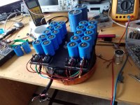
I got some progress on rebuilding my bryston clone, I skipped the entire psu board that came with the kit, I do like some good oldschool psu with brute force, so this is the new psu, its gonna be crc this time, see if I can reduce ripple somewhat, all wirring will be heavy duty solid core copper.
Attachments
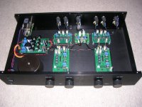
Here are a few pics of my active crossover. The pcbs along the back of the first picture are a power supply, a balanced output module, a balanced input module, and another balanced output module, respectively The two pcbs in the foreground are the 24dB/octave active crossovers. The crossover frequencies are programmable via small single-in-line modules and are set to 3kHz in this case. The inputs and outputs can be balanced or single ended and there are separate level controls for the low and high frequency outputs of each crossover. The modules and their pcbs are all of my own design. The case was chosen to match the size of all my other amps, preamps, etc. Commiserations on the dental pain, I think its the worst kind of pain ( for a man at least ).
Attachments
Now that's what I call a power supply!! I must admit that I'm in two minds about the Bryston clone power supply module too. I have my own designs/pcbs for a soft start module, cap multiplier psu, and speaker protection so I might just use those.
That is very nicely done, I do like meticulously cabling, bravo..! And you made your own pcb with the possibility to change crossover frequency, not bad at all.
Me and the missis are invited out so gotta go, would love a evening at home my jaw is almost numb , guess peoplo are gonna have fun watching me eat.
Me and the missis are invited out so gotta go, would love a evening at home my jaw is almost numb , guess peoplo are gonna have fun watching me eat.
My recommendations are obviously for the big dual channel input board. The small single channel board is a bit trickier. If you look back to my posts showing a revamp of the small input board you'll see I had to get a bit creative. The rca socket I used was a bit of a kluge, it didn't exactly fit the pcb footprint. I couldn't find a switch that fit the rca/xlr position so I simply used two, small, single pole double throw, pcb mount switches. There is no pcb footprint for an xlr connector so I simply soldered in a terminal block.
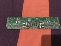
Hi....chalky I bought this input board but it little different from previous version and schematic and bom I received are old one,what is that sw3. Can anyone send schematic and BOM for this board
Attachments
Thanks a lot hschier.....do you have back plate mould pdf ? if so please upload it
Last edited:
The switch sw3 looks it selects between stereo and bridge tied mode. In stereo mode the input board acts like the old one, but in bridge tied mode one channel is inverted. In the latter case any attached dual channel power amplifier becomes a bridge tied mono amplifier with ( in theory ) double the power output. Usually the input proper goes to the non-inverting channel and the inverting channel gets its input from the output of the non-inverting channel ( whose input socket is then disconnected ). However without a board in front of me I can't tell which channel is which and the pcb legend is ambiguous. The physical layout of the Rev 3.0 pcb is different from Rev 2.0 but electrically it looks to be unchanged.
Thanks chalky......another thing to ask from you,I adjusted voltage across R45 around 7-10mv,please explain what are the disadvantages keeping like that without 23mv
Thanks
Thanks
Exactly as I said. In bridged mode the input goes to the right channel and the left channel is inverted. The left and right outputs of the input board go to the left and right inputs of a stereo power amplifier. The loudspeaker is connected across the power amplifier outputs, usually the two red terminals.
If the voltage is too low you'll get crossover distortion. That means this project requires chunky heatsinks ( unfortunately, costwise ).
chunky heatsinks ?...my one is cold at 3/4 volume....what about output gain and ,sound quality/clarity?
You mean it stays cold after running it for a while at 3/4 volume? The heatsinks should warm up a bit with no input; perhaps amplitude will tell us how his amp performed thermally. Don't mess with the gain of the output stage as you could cause the amp to oscillate. Incidentally where did you get the Rev3.0 pcb from?
Single-ended Balanced/RCA Stereo Converter Audio Signal Selector f Bryston 4B-ST | eBay ......little warm at3/4 volume, as I kept 10mv across r45 I thought that it will affect output gain and sound quality (more than 50% low as described in debugging procedure)(above seller sent v3 not the v2 as in pictures)
Last edited:
Turns out that the setup procedure in the debugging instructions is wrong. Bryston recommend that there should be 25mV across a corresponding PAIR of emitter resistors ( i.e. about 12.5mV across a single resistor ) in a fully warmed up amplifier; whereas the debugging instructions suggest 25mV across a SINGLE emitter resistor. So it turns out that your 10mV setting is only a little lower than the Bryston suggested value of 12.5mA.
Attachments
Oh...we have gone wrong way, thanks chalky shearing this...I kindly invite to all to shear own experience on biasing this clone.
Thanks
Thanks
Just been analyzing the output stage before final assembly of my power amp boards. Seems to me that a good match between Q17 and Q18 is important because then the upper and lower halves of the output stage will look very similar regardless of how good the npn to pnp matching of the output devices is. This assumes that all of the npn and all of the pnp output devices are a good match as are all the 2N5401s and 2N5551s in the output stage. Using the devices specified in the BOM makes a Q17/Q18 match difficult, if not impossible. However lets assume that all of the necessary matches can be achieved - what then? It seems that the MJL 21194(npn) has a much lower hfe than the MJL21193(pnp) - certainly true of my batch and also true of fetamps batch. He posted the following table in post #535
Q21 R49 14.3mv pnp
Q22 R48 8.6mv npn*
Q19 R45 13.4mv pnp
Q20 R44 9.3mv npn*
Q25 R57 2.2mv npn*
Q26 R56 7.2mv pnp
Q23 R53 2.8mv npn*
Q24 R52 7.3mv pnp
and as you can see the voltages across the emitter resistors of the npn devices is always much lower than that across the emitter resistors of the pnp devices - indicating a lower hfe for the npn devices. So although the upper and lower halves of the output stage may look electrically similar, the current sharing between between npn and pnp devices won't be too good. The pnp devices will always deliver most of the current to the load.
- Home
- Amplifiers
- Solid State
- Bryston 4B SST clone