Hi all,
I am becoming interested in power amplifiers again, it's been 10 years since last time I built one. This time I want to try out some new ideas I have and see how they turn out.
1. Here's the idea: A well-known simple amplifier circuit is an op-amp driving an emitter-follower buffer. There are some modern nice opamps available such as LME49860 that run off of +-22V rails. If I add an emitter-follower buffer to those opamps, they should be able to output about 18V peak into a speaker. If we put two such amps into a bridged config, that should give 36V peak or about 80W/8ohm. So that is a low parts-count, simple design. Let's see how well it works.
2. I've been using SMT for years, I'd like to experiment with using SMT also in power amplifiers. I even want try out SMT driver transistors. Crazy, I know!
3. I like the idea of having input stage and output stage on two separate PCBs. That will make it more easy to experiment with different topologies. I have more ideas in the pipeline...
I am lucky enough to have an old AP System-1 and a scope to aid in optimizing and troubleshooting. So expect lots of old-fashioned AP plots.
Alright, so here is the LTSpice schematic that I've been playing with for a long time.
Nothing fancy here, just an opamp driving a 2EF with a Vbe multiplier and a bootstrap current source. As simple as it gets.
The opamps are set up for transitional compensation, and with differential gain. The other channel gets the same signal but with inputs swapped.
The opamps have slightly asymmetric supply rails to maximize the output swing since it drives the upper driver transistor.
It manages 36V peak into a 4ohm load before clipping -> 160W/4ohm. This is with 0.25ohm emitter resistors. That simulates to a 20kTHD at 22ppm, not spectacular but not too shabby either.
Attachments
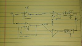
Just a thought here.
How about an opamp configured as a balanced driver.
That balanced driver would feed 2 opamps for your gain.
Each channel of gain will get it's own output buffer.
Then you get your Peak to Peak swing without bridging.
Maybe a bit fidgety, but HEY, that's why we DIY.
How about an opamp configured as a balanced driver.
That balanced driver would feed 2 opamps for your gain.
Each channel of gain will get it's own output buffer.
Then you get your Peak to Peak swing without bridging.
Maybe a bit fidgety, but HEY, that's why we DIY.
Hi! As far as I can see it's a slightly different way of achieving the same thing, it is still a bridged amplifier in the end? But maybe I misunderstand, perhaps a simple schematic would help?
Have a look to LTC6090 and ADA4700-1
These hight voltage opamps make it possible over 100Wrms in 8 ohms, not bridged.
These hight voltage opamps make it possible over 100Wrms in 8 ohms, not bridged.
Last edited:
Yes, those are interesting. Too bad they have such low GBW. The output stage with the MJL3281/1302 is much faster than that, so there is a potential for getting more loopgain with an opamp with higher GBW.
in the 80's using IRF540 , 9540 and LF353 I made a great little 40w car amp doing this.
I used a buffered 555 to provide +20v and -8 volts to the op amps and bias so that it would go easily rail to rail.
output op amps had a gain of 3 driven by a 3rd op amp gain of 6
I used a buffered 555 to provide +20v and -8 volts to the op amps and bias so that it would go easily rail to rail.
output op amps had a gain of 3 driven by a 3rd op amp gain of 6
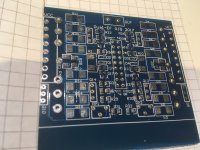
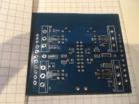
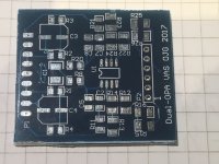
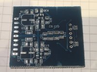
So here are the PCBs I have made at Seeedstudio. Decent quality at prices that were just a fantasy a few years ago.
The output stage PCB contains the two pairs of output transistors and the driver transistors and the Vbe multipliers. I also put in a basic overcurrent protection.
The input stage PCB contains the dual opamp and the bootstrap current sources, and voltage regulator for the opamp. That's it. The two boards will connect with a DIL header.
The output stage PCB is 50mmx65mm and the input stage PCB is just 40mmx35mm.
The next update will be of the assembled PCB.
Attachments
Something like this.
LOL, sorry for the drawing.
Thanks for the drawing, I see what you mean. I think this is still called a bridged amplifier, it is just that you use a preamp-stage to generate the opposite-phase signals and then the power-amp can be just a non-inverting amp. That should work fine too.
in the 80's using IRF540 , 9540 and LF353 I made a great little 40w car amp doing this.
I used a buffered 555 to provide +20v and -8 volts to the op amps and bias so that it would go easily rail to rail.
output op amps had a gain of 3 driven by a 3rd op amp gain of 6
Interesting! With MOSFETs you loose a lot of headroom because of the high Vgs, right? How do you use a 555 as a voltage regulator? Or did you make a switching power supply?
if one changes the topology from emitter follower/source follower to common emitter/common source then the output stage can get very close to the supply rails.Interesting! With MOSFETs you loose a lot of headroom because of the high Vgs, right? How do you use a 555 as a voltage regulator? Or did you make a switching power supply?
using this a mosfET common source output stage can get closer to the supply rails than a BJT stage.
If the low current early stages are run on boosted rails, then rail to rail specification is possible.
Alright! I got something working! I prefer to start new builds slowly, only adding the minimal set of components needed to check if it's working. Then adding more after the intial tests. As I didn't have the MJL3281/1302 transistors yet, I started with the TO-220 D44/D45H11. I also started with a low GBW opamp to make sure it didn't oscillate on the first try.
Initial config:
OPA2132 op-amp
D44H11 / D45H11 output transistors, 0.5ohm emitter resistors
FCX493/FCX593 drivers, 75ohm emitter resistor
Rf = 22k, Rg =3k3.
No compensation capacitor.
+-17V supply voltage
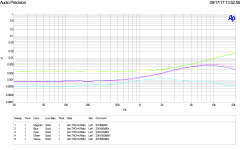
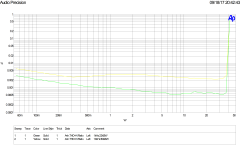
Thankfully no magic smoke came out, and no oscillation! The initial performance is not too bad either. The bias voltage was adjusted for minimal THD+N at 10kHz/1W/80kBW. Which resulted in only 26mA Iq.
Initial config:
OPA2132 op-amp
D44H11 / D45H11 output transistors, 0.5ohm emitter resistors
FCX493/FCX593 drivers, 75ohm emitter resistor
Rf = 22k, Rg =3k3.
No compensation capacitor.
+-17V supply voltage
Thankfully no magic smoke came out, and no oscillation! The initial performance is not too bad either. The bias voltage was adjusted for minimal THD+N at 10kHz/1W/80kBW. Which resulted in only 26mA Iq.
Attachments
Sure, it would work with a single supply rail. Would need to generate a virtual ground then, but that is not a big issue since there is alomst no current going through it. And AC-couple the inputs.
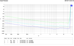
Right now the amp is running DC-coupled and without any DC-servo the output offset is less than 5mV. That is one of the benefits of using opamps for the input stage -> low offset.
Right now the amp is running DC-coupled and without any DC-servo the output offset is less than 5mV. That is one of the benefits of using opamps for the input stage -> low offset.
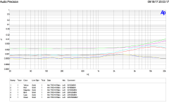
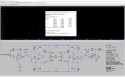
Since it is stable with the OPA2132 without compensation I thought it was time to try a faster opamp. So in goes a LM4562. And lo and behold it is still stable without compensation cap! Bias current is the same as before. Output noise is 19uVrms, un-weighted, 22kHz bandwidth.
Now I'm getting some nice THD results already. 4ppm at 1kHz/22kBW, 10ppm at 10kHz/80kBW.
Now I'm getting some nice THD results already. 4ppm at 1kHz/22kBW, 10ppm at 10kHz/80kBW.
Attachments

Fine.
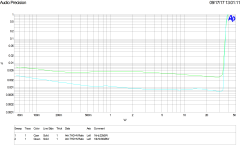
About THD, check at various output levels.
At very low level it can be very good.
At high level it can be very good.
However at some level in between it is not so good.
This output level of worst thd depends of the output stage bias. This comes from gm doubling.
Look for this output level which depends of bias.
By the way, tell me what you think of the " Oliver optimum bias", something regularly mentioned on diy audio.
Hi, didn't you see the THD vs amplitude plots above? Of course I check THD at different output levels.
I started with 26mV across Re as the initial setpoint for the bias current, but this did not result in the lowest THD. Others have found the same, and LTSpice gives the same result. Optimal bias for this configuration is slightly lower. I'll get back to posting some graphs while adjusting to various Iq values.
I started with 26mV across Re as the initial setpoint for the bias current, but this did not result in the lowest THD. Others have found the same, and LTSpice gives the same result. Optimal bias for this configuration is slightly lower. I'll get back to posting some graphs while adjusting to various Iq values.
- Status
- Not open for further replies.
- Home
- Amplifiers
- Solid State
- Bridged Buffered Opamp Amp - a journey