Got it, I didn't know we can right click on the output label/indicator to bring up that box. Easy peezy!Run the simulation. Go to the waveform window and right click inside of it. Select "Add trace". Type the expression.
View attachment 1414549
Cheers
Attachments
That looks about right and gives you a phase margin of about 73 degrees, which is quite typical. If you post the QSPICE files I can double check for you.
But if you did everything correctly, that amplifier shouldn't oscillate during normal circumstances. You can "torture" it by replacing the resistive dummy load with capacitors, inductors and combinations thereof.
But if you did everything correctly, that amplifier shouldn't oscillate during normal circumstances. You can "torture" it by replacing the resistive dummy load with capacitors, inductors and combinations thereof.

Thanks. I have been transistor swapping so I have a few. I'll generate Bode plots for all to see what differences evolve.If you post the QSPICE files I can double check for you.
Cheers
T
If you post the QSPICE files I can double check for you.

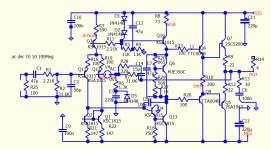
Thanks for your offer to check my work to date, QSPICE file attached. The Vbe bias is a simple affair...
Phase margin is better than 80 degrees; square waves need to be magnified to reveal a nasty on the corner which I hope is benign.
Cheers
Attachments
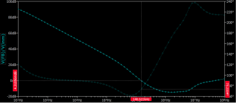
I have attempted a better topology to get a flatter response without the slight drop before rising like my previous attempt. I would like to ask if someone could eyeball the Bode plot to check it. I'm surprised to see the phase margin 133 degrees but it does get rid of the drop seen in my previous plot.
Also, have I understood B Cordell information regarding R9/R12 to be reading 26mV each?
Cheers

Also, have I understood B Cordell information regarding R9/R12 to be reading 26mV each?
Cheers
Attachments
I don't trust your simulation at high frequencies because of where you are breaking the loop. If you move your AC source between your output and the feedback network then I would believe your results. You have to have a large impedance mismatch on both sides of the AC source for all frequencies of interest when you break the loop this way. Looking into the base of a PNP is not a high impedance at some frequency.
Also, it seems dangerous to have the loop gain stop at a gain of one even if you have a large phase margin. Some one with more experience could over rule me on that opinion. I would want a design with some gain margin and some phase margin.
Also, it seems dangerous to have the loop gain stop at a gain of one even if you have a large phase margin. Some one with more experience could over rule me on that opinion. I would want a design with some gain margin and some phase margin.
Thanks for your input. The design is D Self's blameless amp schematic from his book. With the small signal transistors I selected this is the result; Self doesn't specify the parts he used. I'll try the Bode plot capture again using your suggestion.I would want a design with some gain margin and some phase margin.
What figure/number constitutes 'some gain margin and some phase margin'?
Cheers
I am no authority but I would think that a -20 db gain margin and a 30 degree phase margin would be a very stable design. Of course any gain and phase margin is good on paper but you are trying to build in some margin for model variation and layout sensitivity so the circuit will be stable. I am not sure that your circuit is stable because the loop gain of one and the phase of zero are very close together at about 20 MegaHertz.
He mentions MPSA42/MPSA92, MPSA06/MPSA56, in the power amp book, and 2SC2240 in IS current mirror as MPSA42 doesn't work well there.The design is D Self's blameless amp schematic from his book. With the small signal transistors I selected this is the result; Self doesn't specify the parts he used.
Thanks. That part is obsolete and not stocked by DigiKey. Has anyone a suggestion for a suitable replacement.2SC2240
Update:
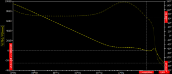
I discovered that by reducing the de-generation resistor value for the top of LTP from R100 to R22 corrected phase margin to 86 degrees from 133!
I don't like the hump to the right. Would this be obviously audible or can I ignore this?
Cheers
I discovered that by reducing the de-generation resistor value for the top of LTP from R100 to R22 corrected phase margin to 86 degrees from 133!
I don't like the hump to the right. Would this be obviously audible or can I ignore this?
Cheers
Attachments
Last edited:
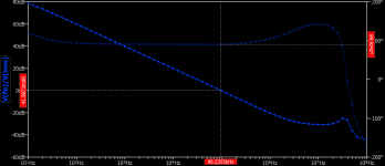
Try experimenting with C14 and R28 to determine effect upon gain at 30MHz. Eg set C14 = 0 for first insight, then experiment with much larger values of R28, etc.
Good luck!
Good luck!
1pF works a treat and, would you believe, increasing the LTP top res to R560 reduces the phase to 90 degrees. Could this be worth keeping to develop some more?set C14 = 0 for first insight,
(there was an error; KSA992 in my previous schematic was wrong)
Cheers
Attachments
- Home
- Amplifiers
- Solid State
- Bode plot reveals instability - solution advice sought