
The easiest way to simulate the open loop gain is to put an AC signal source in series with the output sensing circuit. This allows the DC bias condition to remain intact while running the AC analysis. Then the loop gain will be the (Voltage on one end of the AC source)/(Voltage on the other end of the AC source). The phase is then the difference between the phase measured at both ends of that AC source.
That's a simplified form of the Middlebrook- and Tian-probes. It should work fine if the open-loop output impedance is small compared to the impedance of the feedback network - which is usually the case.
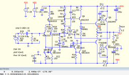
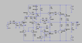
I replaced R4 with 1.33K to get 7 mA through Q8/Q9 but quiescent current on the power rail goes up from 8mA to 300mA so I will consider a different output topology. I had bolted on an output arrangement from B Cordell's example onto D Self's input and VAS. This trouble is all of my own doing . Your advise is helping me learn much and is greatly appreciated. Thank you.Trying this in LTSpice, there's definitely something wrong with the output stage biasing. I'm using KSC1845 and KSA992 for small signal but it should be pretty similar. If I want ~100 mA through Q6/Q4, I need R4 = 1k5, but then the current through Q8/Q9 is ~70 mA, clearly excessive. Try making e.g. R9=R10=100 and R4=1k15, which gives ~100 mA through Q6/Q4 and ~7 mA through Q8/Q9, much more reasonable. Having done that, I get a rather healthy PM of 70 deg and if you remove R2/C14, even better at 83.5 deg.
The purpose of R4 is to set the bias current in Q4 and Q6 and not the bias current in Q8 and Q9. Also, thermal runaway can be avoided by inclusion of the emitter ballast resistors R12 and R17. This output stage is typical of Class A/B outputs and it requires some output bias current to minimize crossover distortion. Other Class A/B bipolar designs will be similar and have to manage the same problems with the bias currents and the thermal matching of transistors.
Yes. I've taken the IP and VAS from Self's blameless design and added an output from diagrams from Cordell's book. I can see this isn't a smart move. I will try a different design.... or just copy Blameless. This is a retirement exercise to kill time LoL! I appreciate the input everyone has given. For clarity, I'll post in a new thread should I try a second attempt. Honestly, it's how to study about what needs to be done to set up for a Bode plot that has me flummoxed and the YouTube videos aren't great for that.This output stage is typical of Class A/B outputs and it requires some output bias current to minimize crossover distortion
Merry Xmas
Terry, the method I used is called a Tian probe, described in detail in the paper I linked above. Some more info here, where it says that QSpice includes an example called Tian.qsch, maybe you can adapt it to your circuit.
The circuit you've put together can work, I'd use a proper Vbe multiplier instead of the diode + resistor for biasing, add emitter degeneration to the VAS and adjust some currents here and there, but the basic topology is fine, it just needs some tweaks.
Merry Xmas to you too!
The circuit you've put together can work, I'd use a proper Vbe multiplier instead of the diode + resistor for biasing, add emitter degeneration to the VAS and adjust some currents here and there, but the basic topology is fine, it just needs some tweaks.
Merry Xmas to you too!
Yes, thanks. It did consider VBE multpier at one point like D Self's examples but I didn't want to copy others' intellectual property too much. I started with the intension to build a Class B amp which I believe has wide crossover distorsion area making biasing easier/forgiving. My first amp purchase, in 1979, was NAD 3020 - Class B can sound good.the basic topology is fine, it just needs some tweaks.
A bit off topic....Once built and tested I plan to produce boards to sell either directly to DIY builders or let Mens Shed accociations procure boards themselves to sell populated boards to generate money for local charities. My personal aim is to donate profits to onedollarglasses recently renamed goodvision https://goodvision.org/.
Merry Christmas
Please advise should this be better posted in a new thread.
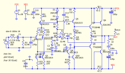
In seeking an alternative solution to a Vbe multiplier I tested this (attached file) with QSPICE. The output is unorthodox but, at a glance, sine and square wave measurements look normal. Attributes: B Cordell, Designing Audio Power Amplifiers; http://www.redcircuits.com/Page150.htm
I deduce R9 /10 resistors turn on the outputs only after the drivers are conducting about 45mA.
None of this might be good and I'd welcome feedback.
Cheers
Attachments
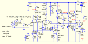
Is there some connection via label that I'm not seeing or is there nothing driving Q6 and Q7?
VBE multipliers have been used all over the place for many decades. I'm quite sure you can use them, for DIY or commercially, without violating anyone's patent or other intellectual property rights.
VBE multipliers have been used all over the place for many decades. I'm quite sure you can use them, for DIY or commercially, without violating anyone's patent or other intellectual property rights.
+1, the very first amplifier kit I ever built in the late 70's already had a Vbe multiplier in it. Every book I have on audio power amplifier design uses it without explicit attribution: Self, Cordell, Duncan, Slone, J. L. Hood... Since you're planning to make PCBs and sell them, you want something that will not self-destroy due to thermal runaway, so it would be prudent to use a Vbe multiplier with a TO-126 transistor (e.g. another TTC004B) that can easily be mounted on the main heatsink for proper thermal compensation.
I don't know who claims that that's a Cordell design but I can't find anything like it in his book, on page 150 or elsewhere. You were much more on the right track with the previous design...
I don't know who claims that that's a Cordell design but I can't find anything like it in his book, on page 150 or elsewhere. You were much more on the right track with the previous design...
I forgot to add that at N04 it measures 50mV to indicate that's what D Self suggests is optimal.label
I deduce that Q6 /7 get turned on when the drivers are conducting enough...just around 45+mA?
I appreciate your input, cheers.
Last edited:
"Shown also is a high-frequency R-C filter in theCordell design (p208 onward)
rail between the output transistors and the preceding driver stages. This acts in two
ways. First, it breaks the feedback path via the common rail at high frequencies. Second,
it acts as a Zobel network on the supply rail to dampen resonances there. This R-C filter
is an opportunity for stabilization that many designers overlook."
To date, my attempt to change the Vbe so as not to look like it's copied from D Self's Blameless circuit has not been successful but I concur with what you write.
Might the inclusion of output transistor emitter resistors help minimise thermal runaway?
Might placing the diode across a transistor collar then calibrating R4 after soak test also work?
Cheers
Last edited:
There is nothing to supply base current to Q6 and Q7, so I don't see how they could turn on (unless you drive them in avalanche mode by applying more than 230 V between collector and emitter).
Amplifiers based on the 1950's Lin circuit (such as those of Self) are all variants on a theme.
To date, my attempt to change the Vbe so as not to look like it's copied from D Self's Blameless circuit has not been successful but I concurr with what you write.
Amplifiers based on the 1950's Lin circuit (such as those of Self) are all variants on a theme.
Look at the orientation of the output transistors and the connection to the drivers Terry, the one in the redcircuits link is a completely different topology...
Thank you for reading my posts and highlighting my errors. I've removed what I needn't have added.different topology.
I should persevere with the Vbe over the holidays as the Redcircuit design might need one...it's simplicity makes me think the crossover region might be wide and forgiving as mentioned by D Self writes about Class B emotter follower.
Attachments
Tutorial on the Tian probe on youtube:
and the design can be found in the examples>educational files of LTSpice, Loopgain2
Hey guys,
Happy New 2020 to you all!
With this post I wanted to announce that I am starting Youtube channel on the design of audio power amplifiers. The content will be completely educational, and will cover the foundations of amplifier design and as well as the design of a best in class audio power amplifier. Searching Youtube, I noticed this has not been done before, so I wanted to give it a shot.
The plan is to keep updating this first post as an index of all the material as it gets published. The plan is to crank a video a week, so we'll see. I am pretty excited about this, so...
- sandrohv
- Replies: 204
- Forum: Solid State
and the design can be found in the examples>educational files of LTSpice, Loopgain2
Thanks, Cabrio and a happy new year. I replaced the drivers with the KSA992 / 1845 pair. Their higher gain made biasing configuration much easier. Vbe multiplier still in progress.Trying this in LTSpice, there's definitely something wrong with the output stage biasing. I'm using KSC1845 and KSA992 for small signal but it should be pretty similar. If I want ~100 mA through Q6/Q4, I need R4 = 1k5, but then the current through Q8/Q9 is ~70 mA, clearly excessive. Try making e.g. R9=R10=100 and R4=1k15, which gives ~100 mA through Q6/Q4 and ~7 mA through Q8/Q9, much more reasonable. Having done that, I get a rather healthy PM of 70 deg and if you remove R2/C14, even better at 83.5 deg.
Cheers
Attachments
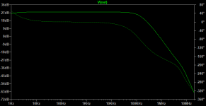
Thank you for attaching the LTSpice sim file. I've tried to run it in LTSpice but, as yet, I can't debug why it returns Failed Analysis : Matrix is missing. I had hoped to test by how much to increase the VAS degeneration res as you suggested might be a suitable tweak. Should you still have the bode plot file would it be possible to post here it for me to learn from?I attach the stability simulation in LTSpice in case someone wants to give it a try.
Cheers,
Terry
- Home
- Amplifiers
- Solid State
- Bode plot reveals instability - solution advice sought