Looks good, but bear in mind that you MUST disable the ultrasonic filter when testing for stability with squarewaves.
Cheers,
Bob
Cheers,
Bob
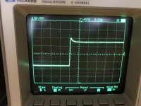
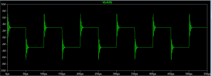
Ok, thanks. Here's the test again with the input filter bypassed.
So, evidently, a little overshoot. I'd like to see less ringing, but even a 0.01uF capacitor is a pretty hefty reactive load. Going up to 0.1uF is a real stress test. I'm thinking this is acceptable, if not optimal. The good news is, the amplifier didn't break into oscillation. I'm not really clear if the overshoot is something inherent to TPC. I also wonder if some of the ringing is from the output inductor.
The other encouraging thing is the amp didn't show any signs of freaking out when driven with a fast-rising input signal and no filtering. The input stage was probably slewing without the filter, but I didn't take the time to check just now. In earlier tests, I did force it to slew and nothing bad happened.
I took this thing straight from SPICE without trying to tweak the compensation on the bench, so it's bound to be off and could be improved. It's really lazy of me, but I don't like to grind up my prototypes so I rush to put them into a nice box, where it's really hard to go in and change things after the fact.
I did the same test on my Topping A30 Pro which is reputed to be the greatest thing since sliced bread. I did not try to bypass any input filtering, just went straight into the input jacks. The result was very similar to my first photos for what it's worth (probably not much).
Attachments

Last edited:
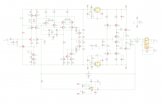
Here's the schematic. I hesitated to show this to you because I didn't want to embarrass myself. 🙂
Your front-end, IMHO, is really really thoughtfully designed and has several features that elevate it above similar circuits. The common-mode control loop is very clever and, aside from the benefits you outline in your paper, it does a great job of locking in the input stage operating point. The clamping is also very nice. From the get-go, this amplifier hasn't given me a lick of trouble. I can't say the same for the "Blameless" design I tried earlier.
One thing I know I got wrong is the compensation network. You can probably tell what I was thinking, but it was only after it was done that I realized, "Wait, the signals at the VAS output aren't differential." So that totally hoses my notion of a balanced, floating compensation network. The funny thing is, the SPICE Bode plot is textbook-perfect this way. When I realized my error, I went back and tried to design a single-ended compensation network, but I couldn't find a scheme that simulated better than what I have here. Eventually, I will try to figure out analytically what I've actually created.
I want to emphasize that I'm not a professional and make no claims with to respect to my design expertise. This has been a learning exercise.
Attachments
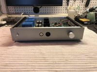
That's really nice looking, a clean, tidy (happy) chassis,
is a good sounding and testing chassis.
Few surprises there.
I love the symmetry and layout... KUDOS!
Thanks very much. I may not know what I'm doing technically, but I've gotten better at building boxes.
Attachments
Ok, thanks. Here's the test again with the input filter bypassed.
So, evidently, a little overshoot. I'd like to see less ringing, but even a 0.01uF capacitor is a pretty hefty reactive load. Going up to 0.1uF is a real stress test. I'm thinking this is acceptable, if not optimal. The good news is, the amplifier didn't break into oscillation. I'm not really clear if the overshoot is something inherent to TPC. I also wonder if some of the ringing is from the output inductor.
The other encouraging thing is the amp didn't show any signs of freaking out when driven with a fast-rising input signal and no filtering. The input stage was probably slewing without the filter, but I didn't take the time to check just now. In earlier tests, I did force it to slew and nothing bad happened.
I took this thing straight from SPICE without trying to tweak the compensation on the bench, so it's bound to be off and could be improved. It's really lazy of me, but I don't like to grind up my prototypes so I rush to put them into a nice box, where it's really hard to go in and change things after the fact.
I did the same test on my Topping A30 Pro which is reputed to be the greatest thing since sliced bread. I did not try to bypass any input filtering, just went straight into the input jacks. The result was very similar to my first photos for what it's worth (probably not much).
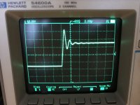
Nice photos. What is the frequency of the ringing in the 3rd photo?
Cheers,
Bob
Here's the schematic. I hesitated to show this to you because I didn't want to embarrass myself. 🙂
Your front-end, IMHO, is really really thoughtfully designed and has several features that elevate it above similar circuits. The common-mode control loop is very clever and, aside from the benefits you outline in your paper, it does a great job of locking in the input stage operating point. The clamping is also very nice. From the get-go, this amplifier hasn't given me a lick of trouble. I can't say the same for the "Blameless" design I tried earlier.
One thing I know I got wrong is the compensation network. You can probably tell what I was thinking, but it was only after it was done that I realized, "Wait, the signals at the VAS output aren't differential." So that totally hoses my notion of a balanced, floating compensation network. The funny thing is, the SPICE Bode plot is textbook-perfect this way. When I realized my error, I went back and tried to design a single-ended compensation network, but I couldn't find a scheme that simulated better than what I have here. Eventually, I will try to figure out analytically what I've actually created.
I want to emphasize that I'm not a professional and make no claims with to respect to my design expertise. This has been a learning exercise.
Thank you for your kind words about my IPS/VAS. For those who don't know, that is the IPS/VAS I used in my MOSFET power amplifier with error correction back in circa 1983. The JAES paper is available on my website at cordellaudio.com.
Cheers,
Bob
Nice photos. What is the frequency of the ringing in the 3rd photo?
Cheers,
Bob
It looks like the ringing is somewhere around 300kHz, and to be honest in my opinion it will oscillate when loaded with a real life load. He should do something with the compensation, focus a bit more on stability instead of trying to force a low THD.
Just my thought.
Stein
Yes, it's around 300 kHz, evidently.
I'm not sure what you mean by "real life.' This is a very demanding load. No headphone is even close to being this capacitive. And technically it's not oscillation, since it isn't sustained.
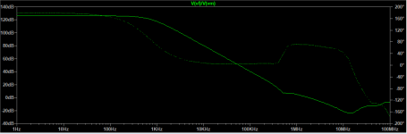
I ran a SPICE simulation and the predicted behavior is similar, though at a higher frequency. The Bode plot shows a weird phase kink but the margins at the ULG are fine. I don't have a network analyzer, so no way to really investigate this on the bench. Some things aren't evident from a Bode plot. To understand this behavior, I would need to do a much deeper analysis and I don't have the technical insight to do that right now. It's not clear to me that this is a real-world problem, overdriving the amplifier with the input filter disabled and a big low-ESR capacitor on the output.
Playing with compensation network values with the simulated 0.1uF load capacitance is inconclusive. Increasing the value of the output inductor improves things in the simulation, and removing it entirely causes the amplifier to break out into full-blown oscillation. This doesn't surprise or necessarily worry me. I put the inductor in there for a reason. The simulated open-loop gain of this amplifier is around 135 dB and the phase falls to about three degrees at midband due to TPC. I was pushing things deliberately with this design to see what I could get away with. It wasn't just a naive attempt to get ultra-low distortion.
The simulation also predicts the overshoot with just the resistive load. Investigation shows the VAS is overloading due to the fast-rising signal. You can always overdrive an amplifier. The ultrasonic filter is an important feature.
The amplifier sounds really nice. It shows no signs of instability with typical loads and is dead quiet. I'm not representing it as anything other than an experiment to see how many transistors, and how much gain I could throw at the problem without building a radio transmitter. I've achieved my goal and am very happy with it overall.
I'm not sure what you mean by "real life.' This is a very demanding load. No headphone is even close to being this capacitive. And technically it's not oscillation, since it isn't sustained.
I ran a SPICE simulation and the predicted behavior is similar, though at a higher frequency. The Bode plot shows a weird phase kink but the margins at the ULG are fine. I don't have a network analyzer, so no way to really investigate this on the bench. Some things aren't evident from a Bode plot. To understand this behavior, I would need to do a much deeper analysis and I don't have the technical insight to do that right now. It's not clear to me that this is a real-world problem, overdriving the amplifier with the input filter disabled and a big low-ESR capacitor on the output.
Playing with compensation network values with the simulated 0.1uF load capacitance is inconclusive. Increasing the value of the output inductor improves things in the simulation, and removing it entirely causes the amplifier to break out into full-blown oscillation. This doesn't surprise or necessarily worry me. I put the inductor in there for a reason. The simulated open-loop gain of this amplifier is around 135 dB and the phase falls to about three degrees at midband due to TPC. I was pushing things deliberately with this design to see what I could get away with. It wasn't just a naive attempt to get ultra-low distortion.
The simulation also predicts the overshoot with just the resistive load. Investigation shows the VAS is overloading due to the fast-rising signal. You can always overdrive an amplifier. The ultrasonic filter is an important feature.
The amplifier sounds really nice. It shows no signs of instability with typical loads and is dead quiet. I'm not representing it as anything other than an experiment to see how many transistors, and how much gain I could throw at the problem without building a radio transmitter. I've achieved my goal and am very happy with it overall.
Attachments
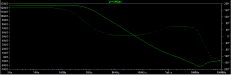
Attached are SPICE Bode plots for the amplifier with a 32 Ohm load, and then 32 Ohms in parallel with 0.1uF. The ringing in the plot from the previous post is at about 480kHz and corresponds to the kink in the response I mentioned.
I'm very happy with the first Bode plot. It's textbook-perfect. Phase margin is about 62 degrees and gain margin is 23 dB. I have no technical insight into the meaning of the change between the two plots, except to say that the "kink" suggests a resonance of some sort. If anyone has any ideas, I would be happy to hear them. As I said, I couldn't find a way to clean this up in the simulation by changing the compensation network values. I will try some other things when I get a chance.
I'm very happy with the first Bode plot. It's textbook-perfect. Phase margin is about 62 degrees and gain margin is 23 dB. I have no technical insight into the meaning of the change between the two plots, except to say that the "kink" suggests a resonance of some sort. If anyone has any ideas, I would be happy to hear them. As I said, I couldn't find a way to clean this up in the simulation by changing the compensation network values. I will try some other things when I get a chance.
Attachments
All amps that have a capacitive load will ring when driven with a square wave. This will be caused by the load inductance (output coil, cable inductance) and any capacitive loading.
You can check if this is what's happening simply by employing fo = 1/rt(2*pi*L*C). If it computes your ringing frequency correctly, then that's what's causing it. If it does not, it may well be a stability issue.
The kink in the second plot is typical of the resonance dip you get from LC ringing and is quite normal.
(See slide 6 here Output L_1)
Last edited:
Here's the schematic. I hesitated to show this to you because I didn't want to embarrass myself. 🙂
Your front-end, IMHO, is really really thoughtfully designed and has several features that elevate it above similar circuits. The common-mode control loop is very clever and, aside from the benefits you outline in your paper, it does a great job of locking in the input stage operating point. The clamping is also very nice. From the get-go, this amplifier hasn't given me a lick of trouble. I can't say the same for the "Blameless" design I tried earlier.
One thing I know I got wrong is the compensation network. You can probably tell what I was thinking, but it was only after it was done that I realized, "Wait, the signals at the VAS output aren't differential." So that totally hoses my notion of a balanced, floating compensation network. The funny thing is, the SPICE Bode plot is textbook-perfect this way. When I realized my error, I went back and tried to design a single-ended compensation network, but I couldn't find a scheme that simulated better than what I have here. Eventually, I will try to figure out analytically what I've actually created.
I want to emphasize that I'm not a professional and make no claims with to respect to my design expertise. This has been a learning exercise.
Fix your servo, with the values in the drawing you'll have some low frequency peaking. Make C14=1uF
I cribbed that servo direct from Salas' DCG3. Didn't even bother to simulate it. I will look into your suggestion for the next go-round. Thanks.
All amps that have a capacitive load will ring when driven with a square wave. This will be caused by the load inductance (output coil, cable inductance) and any capacitive loading.
You can check if this is what's happening simply by employing fo = 1/rt(2*pi*L*C). If it computes your ringing frequency correctly, then that's what's causing it. If it does not, it may well be a stability issue.
The kink in the second plot is typical of the resonance dip you get from LC ringing and is quite normal.
(See slide 6 here Output L_1)
Thanks for the link. You pretty much nailed what I'm seeing.
I played around in SPICE and couldn't find anything wrong with the compensation or overall gain structure. Removing the inductor completely, the 100nF capacitor introduces a pole that cancels the zero in the TPC network, and of course the amplifier goes unstable. There's nothing you can do about that except dominant-pole compensate the living daylights out of it, and lose all your bandwidth and NFB.
Removing the 10 Ohm resistor in parallel with the inductor sharpens the "kink" into a classic LC resonance. Changing the value of the inductor changes the frequency of the ringing. The amplifier is unconditionally stable with the inductor in place, and, as you say, it makes the gain and phase margin virtually constant versus load capacitance. The ringing is the price you pay for load isolation.
A 10 Ohm resistor in series with the output, after the feedback, does an even nicer job, but I want low output impedance.
Your slides give me confidence I don't need to worry about it.
@ Bob Cordell
Dear Bob
While reading your book (second edition routledge) I found an alternative to zener gate protection for mosfets in page 341.
I find the natural current limiting provided by the flying catch diodes apealing but could not make it work in my latest lateral mosfet power amp.
Does this method work with laterals ?
Attachments
Here's the schematic. I hesitated to show this to you because I didn't want to embarrass myself. 🙂
Your front-end, IMHO, is really really thoughtfully designed and has several features that elevate it above similar circuits. The common-mode control loop is very clever and, aside from the benefits you outline in your paper, it does a great job of locking in the input stage operating point. The clamping is also very nice. From the get-go, this amplifier hasn't given me a lick of trouble. I can't say the same for the "Blameless" design I tried earlier.
One thing I know I got wrong is the compensation network. You can probably tell what I was thinking, but it was only after it was done that I realized, "Wait, the signals at the VAS output aren't differential." So that totally hoses my notion of a balanced, floating compensation network. The funny thing is, the SPICE Bode plot is textbook-perfect this way. When I realized my error, I went back and tried to design a single-ended compensation network, but I couldn't find a scheme that simulated better than what I have here. Eventually, I will try to figure out analytically what I've actually created.
I want to emphasize that I'm not a professional and make no claims with to respect to my design expertise. This has been a learning exercise.
Hi All,
Bobs book has info on simulating thermal circuits for power amps in Ch 17, eg, Fig 17.6 and thermal bias stability with emitter resistors (S17.6) and a thermal model for the ThermalTraks (Fig 17.21). For those who would like to do more electrothermal simulations I have made available 5 subcircuits "widgets" that convert the following models to be electrothermal: BJT, MOSFET, JFET, Diode, and IGBT. They were announced in this thread https://www.diyaudio.com/community/threads/better-power-mosfet-models-in-ltspice.266655/post-6885269 with a tutorial and demo jigs.
Also I have some files (attached) as a demo for the standard topology similar to Fig 3.2 in Bob's book which is the 2nd version with input stage degeneration.

I have used the circuit posted by ctrlx here as I was interested to see how hot the single output stage would get with a single output pair of MJL's with a likely heatsink for a 100W amp. My sim shows Tj gets to about 100C and the heatsink 75C.

The simulation was for 30 seconds but in reality it takes about half an hour for the heatsink to stabilize. The time constants in my simulation have been compressed by a factor of about 1000 so the simulation doesn't take for ever. My PC took 370 seconds to run, so if real time constants were used it would take 100 hours and the drive used 1.4GB for plotting so maybe 140GB without time scaling.
The first 10 seconds is with no signal so you can see the amp warming up to idle current of 105mA. It starts at 90mA. With the signal the idle current becomes 123mA which is a quite good result showing the spreader has about the right thermal attenuation. To view FFT you enter Start Time and End Time and click Specify Time range typically covering 10 cycles from zero crossing times, or preselect a range in the plot window and click Use Current Zoom Extent. BTW the .Four card doesn't give anything meaningful with this type of simulation.
I'll cover the compensation I chose for this simulation in a following post.
I've tried to make these widgets intuitive and as easy as possible to use. Any help, queries, comments, bug reports and/or suggestions are all very welcome. And if there is enough interest a new thread will be started, to not hijack this one.
Bobs book has info on simulating thermal circuits for power amps in Ch 17, eg, Fig 17.6 and thermal bias stability with emitter resistors (S17.6) and a thermal model for the ThermalTraks (Fig 17.21). For those who would like to do more electrothermal simulations I have made available 5 subcircuits "widgets" that convert the following models to be electrothermal: BJT, MOSFET, JFET, Diode, and IGBT. They were announced in this thread https://www.diyaudio.com/community/threads/better-power-mosfet-models-in-ltspice.266655/post-6885269 with a tutorial and demo jigs.
Also I have some files (attached) as a demo for the standard topology similar to Fig 3.2 in Bob's book which is the 2nd version with input stage degeneration.
I have used the circuit posted by ctrlx here as I was interested to see how hot the single output stage would get with a single output pair of MJL's with a likely heatsink for a 100W amp. My sim shows Tj gets to about 100C and the heatsink 75C.
The simulation was for 30 seconds but in reality it takes about half an hour for the heatsink to stabilize. The time constants in my simulation have been compressed by a factor of about 1000 so the simulation doesn't take for ever. My PC took 370 seconds to run, so if real time constants were used it would take 100 hours and the drive used 1.4GB for plotting so maybe 140GB without time scaling.
The first 10 seconds is with no signal so you can see the amp warming up to idle current of 105mA. It starts at 90mA. With the signal the idle current becomes 123mA which is a quite good result showing the spreader has about the right thermal attenuation. To view FFT you enter Start Time and End Time and click Specify Time range typically covering 10 cycles from zero crossing times, or preselect a range in the plot window and click Use Current Zoom Extent. BTW the .Four card doesn't give anything meaningful with this type of simulation.
I'll cover the compensation I chose for this simulation in a following post.
I've tried to make these widgets intuitive and as easy as possible to use. Any help, queries, comments, bug reports and/or suggestions are all very welcome. And if there is enough interest a new thread will be started, to not hijack this one.
Attachments
Last edited:
Re: Compensation for the electrothermal demo
The original circuit I used by ctrlx here used Miller Input Compensation, 10pF from the VAS collector to the inverting input. This gave a closed loop rolloff at 1.1MHz using laterals. The SR is about 30V/us. Bob's Fig 3.2 is similar with 500kHz and 37V/us.
When I checked the ctrlx version for clip recovery I found I needed to increase the compensation capacitor to at least 100pF to get a smooth recovery with no ringing and ideally 220pF. But with 220pF the rolloff is 66kHz and SR 6V/us. Also THD increases from 0.004% at 100W 1kHz to 0.033% or nearly 10 times higher.
For those who are experienced in compensation is this what happens in most standard topology amps? I tried using straight Miller compensation and when I chose the value for the same open-loop rolloff as for a 220pF IMC (which was 390pF) I got almost the same clip recovery and almost the same closed loop rolloff.
It looks like compensating for a smooth clip recovery requires 10 times the capacitance giving around 10 times the THD and 1/10th the slew rate and bandwidth. So is it common practice to ignore a smooth clip recovery and just go for good stability and minimal THD?
As for my method of checking for ringing, this plot below shows my MJL version with a 100pF Miller capacitor and 100pF+100R shunting the VAS. Clip recovery ringing has gone and would otherwise appear the the arrow in the derivative plot of Vout. If you run the circuit (see previous post) and reduce Cdom you can then see a sharp spike at the recovery.

As an aside, the my MJL version had different issues to the original lateral version to get it stable, hence the inclusion of the 100pF+100R shunting the VAS.
Also, I found the 470nF (C4) shunting the Locanthi resistor (R19) did not help either the MJL or lateral versions, so I disabled it in my sims; it didn't change the slew rate or affect cross-conduction when slew limiting.
I also tried a BAT54 across b-c of the CCS (Q8) but I did not notice much improvement in the clip recovery plot using the above plot method.
Nothing seems as easy as it looks at first .
.
The original circuit I used by ctrlx here used Miller Input Compensation, 10pF from the VAS collector to the inverting input. This gave a closed loop rolloff at 1.1MHz using laterals. The SR is about 30V/us. Bob's Fig 3.2 is similar with 500kHz and 37V/us.
When I checked the ctrlx version for clip recovery I found I needed to increase the compensation capacitor to at least 100pF to get a smooth recovery with no ringing and ideally 220pF. But with 220pF the rolloff is 66kHz and SR 6V/us. Also THD increases from 0.004% at 100W 1kHz to 0.033% or nearly 10 times higher.
For those who are experienced in compensation is this what happens in most standard topology amps? I tried using straight Miller compensation and when I chose the value for the same open-loop rolloff as for a 220pF IMC (which was 390pF) I got almost the same clip recovery and almost the same closed loop rolloff.
It looks like compensating for a smooth clip recovery requires 10 times the capacitance giving around 10 times the THD and 1/10th the slew rate and bandwidth. So is it common practice to ignore a smooth clip recovery and just go for good stability and minimal THD?
As for my method of checking for ringing, this plot below shows my MJL version with a 100pF Miller capacitor and 100pF+100R shunting the VAS. Clip recovery ringing has gone and would otherwise appear the the arrow in the derivative plot of Vout. If you run the circuit (see previous post) and reduce Cdom you can then see a sharp spike at the recovery.
As an aside, the my MJL version had different issues to the original lateral version to get it stable, hence the inclusion of the 100pF+100R shunting the VAS.
Also, I found the 470nF (C4) shunting the Locanthi resistor (R19) did not help either the MJL or lateral versions, so I disabled it in my sims; it didn't change the slew rate or affect cross-conduction when slew limiting.
I also tried a BAT54 across b-c of the CCS (Q8) but I did not notice much improvement in the clip recovery plot using the above plot method.
Nothing seems as easy as it looks at first
.Most interesting post. Thank you for the enlightenmentSome loudspeakers are more sensitive to variations in source impedance (damping factor) than others. Any speaker using passive 4th-order crossover filters, or the acoustical version, which is a vented box, is going to be more sensitive to source impedance than a speaker using low-Q alignments.
For the raw driver, damping factor doesn't matter that much, since voice coil resistance (Re) is in series with the inductors in the crossover, speaker wiring resistance, and the source impedance of the power amplifier. With a typical voice-coil DCR of 6 ohms, inductor resistance anywhere from 0.1 to 0.5 ohms, and speaker cable resistance anywhere from 0.05 (very unusual) to 0.3 ohms (for long runs), an amplifier source resistance much lower than 0.2 ohms (which is a damping factor of 80) is basically wasted. From the perspective of the driver, it is the ratio between DCR and all the source impedances that matter - and once this ratio is much beyond 40 or so, there's not much difference to the response or distortion of the driver.
4th-order crossovers (electrical) or 4th-order (vented) cabinets are a little more touchy, simply because they are 4th-order filters, and are more sensitive to small parameter variations. Nearly all the filter damping is coming from the power amplifier, not resistive terms in the filter. Unfortunately, in loudspeaker drivers, the Q is not that well controlled.
The cone mass is very predictable; 1% repeatability is common and expected. Likewise, the number of turns in the gap is well-controlled, since this is wound on a machine with a turns counter. Compliance is not well-controlled, with a 20~30% shift during the break-in process. But compliance shifts fortunately have little effect on cabinet alignment or crossover behavior.
It's the BL product that is troublesome. BL product are the turns multiplied by the Teslas of field strength in the gap; L stands for length of wire, which is well controlled, but the effective B field that the VC sees is quite another matter. Overhung voice coils, by far the most common, have a significant portion outside the gap, and the magnetic field lines are not well-controlled in the region (in the gap the field lines are parallel and reasonably equally spaced). Move the voice coil a bit (excursion) and the different portions of the VC are exposed to the nonlinear field structure above and below the gap (which are asymmetric). Various attempts have been made to linearize the out-of-gap field, but even the complex systems are far less linear than what's in the gap - and overhung VC always have mixture of turns exposed to the fields inside and outside the gap. Not only that, the VC is continually moving, so low frequency excursions intermodulate higher frequencies.
The old-school Altec and Lowther approach is an underhung VC, which later used by TAD for their Alnico-magnet woofers. This is inherently far more linear, basically the loudspeaker equivalent to Class A operation. But once the VC starts to leave the gap to get that boom-boom bass everyone loves, then linearity goes downhill quickly. Overhung VC speakers are cheaper to build, which is another reason they dominate 99% or more of the market. Guitar speakers are equal-hung, which gives the most efficiency, but also the most distortion, since any movement at all makes the VC leave the gap.
So unfortunately BL, and therefore Qts, is not a well-controlled, linear parameter. It is not an accident that the specified Qts is what driver manufacturers call a "small-signal" parameter, which is a cute way of saying it is level-dependent. What you get at 40 dB is not the same as what you get at 90 dB. This is inherent to the technology, sorry.
This variation in BL and Q under dynamic conditions has implications for cabinet and crossover design. Since BL and Q are not well-controlled, it calls into question the wisdom of high-order alignments that rely on precise control of the filter elements. Driver mass, cabinet volume, and the passive components in a crossover are well-defined, but cone compliance, BL, and Qts are not, and shift under dynamic conditions in a complex way, with significant stored energy in the spring-return of the spider and high-Q resonances and standing waves of the diaphragm and interior cabinet volume.
There are a lot of high-end speakers these days that have high-order crossovers in vented boxes; they will be much more sensitive to source Z of the amplifier than speakers that use closed-boxes, or resistive vents, and also have low-Q crossovers (2nd-order or lower). But relying on the amplifier to magically "straighten out" what's happening in the VC gap isn't going to happen; the entire amplifier-speaker interface rests on the field-line structure in the gap, and how linearly it moves the voice coil. If the field lines are curved and distorted, then the amp-speaker interface has to follow along, and behave the same way. The entire amplifier is always seen through the prism of the field lines that drive the voice coil. This is true of all magnetically driven loudspeakers, regardless whether they are planar, ribbon, or conventional.
This is where the great Class AB debate about bias stability under dynamic conditions has relevance for loudspeakers. A transistor amplifier is making its transition out of Class A (around a watt or so) at about the same level that a loudspeaker is leaving what is considered the "small-signal" region - in other words, anywhere from 85 to 92 dB SPL at one meter, depending on typical efficiencies. It also tells us that high-efficiency speakers in the 96+ dB region may be a lot less forgiving of dynamic bias shift than less-efficient speakers.
Bob, I saw the presentation of the BC-1 amplifier. I dialed the model of this amplifier and I had a number of questions. May I ask them here?
with best regards,
Peter
with best regards,
Peter
- Home
- Amplifiers
- Solid State
- Bob Cordell's Power amplifier book