Hi Harry,
Thanks for that. I use LTSpice now - so will study the methods. I agree that the models from the manufacturers are not very accurate, as i have notified them of errors, they agreed the error, but the model did not change on their website.
Regards,
Shadders.
Thanks for that. I use LTSpice now - so will study the methods. I agree that the models from the manufacturers are not very accurate, as i have notified them of errors, they agreed the error, but the model did not change on their website.
Regards,
Shadders.
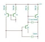
An emitter follower inserted between the input stage and the VAS transistor does the same and even proves to be better for the overall performances.Keeping VAS transistor base-collector voltage more-or-less constant eliminates effects of its non-linear base-collector capacitance
Attachments
Last edited:
The cure to all this of course is submitting your book for print-on-demand.
Jan
I ordered a Linear audio print on demand book last week as a xmas present for a friend who was coming over from USA. I was very suprised that it arrived within 4 days of the order. I now want to find a bookshop with a POD machine so I can buy a book and watch it get made in front of me 🙂
VAS Stability ?
Hi,
Working through the small signal equivalent of a cascaded VAS, and cascode transistor before the output stage, what seems to be a possible concern is that the entire circuit begins to approximate an R-C phase oscillator.
I still have to progress my amplifier where I used a double instead of a triple for the output stage, which oscillated at 120kHz approx, and modifying the LTP output pole (using series R-C) stopped the oscillation. Adding the second pair of output transistors caused the amplifier to oscillate again at approx 70kHz.
So, what is the preferred method/order to eliminate oscillation :
For my PCB design I used surface mount and crammed everything onto the board, but did use both sides. Will the potential PCB track routes with stray capacitances always be an issue for MHz oscillation, and therefore, ensuring that the PCB has the component positions for adding stability aspects (VAS zobel) be the best approach ?.
Regards,
Shadders.
Hi,
Working through the small signal equivalent of a cascaded VAS, and cascode transistor before the output stage, what seems to be a possible concern is that the entire circuit begins to approximate an R-C phase oscillator.
I still have to progress my amplifier where I used a double instead of a triple for the output stage, which oscillated at 120kHz approx, and modifying the LTP output pole (using series R-C) stopped the oscillation. Adding the second pair of output transistors caused the amplifier to oscillate again at approx 70kHz.
So, what is the preferred method/order to eliminate oscillation :
- Modify the VAS circuit resistances to obtain stability ? Or move it up in frequency ?
- Use higher value base stopper resistors between the driver and output stage ?
- Add the zobel network to the VAS output ? (Bob’s book 2nd Ed, chapter 13). For this option, Doug Self used a capacitor without a resistor, which affected the THD for high capacitor values (500pF and larger).
- For the cascode, set the bias voltage using resistances as opposed to a zener diode such that zener diode capacitance does not affect the circuit.
For my PCB design I used surface mount and crammed everything onto the board, but did use both sides. Will the potential PCB track routes with stray capacitances always be an issue for MHz oscillation, and therefore, ensuring that the PCB has the component positions for adding stability aspects (VAS zobel) be the best approach ?.
Regards,
Shadders.
The VAS zobel worked for me. My VAS is darlington but not cascode. Output is 2 pair of parallel devices and is EF2 (no predrivers). The amp was quite stable running from the drivers without the power transistors connected, but connecting the output caused problems. The zobel took care of it. I can do all of the suggested things to the feedback loop (cut R in half, add C to ground) and it is stable. Generator does not go over 2 MHz so I can't look for peaking above that.
Hi Fred,
Thanks for the info. In checking the cascode transistor Cje, it is 3nF, which is quite a high value, and Cjc is 300pF. So my interpretation here is that low values resistances will cause the pole to move up in frequency, and high value resistances in the VAS will cause the pole to move lower in frequency. Can yourself or anyone else confirm ?
I have not used a resistor between the first VAS transistor collector and ground. So, this option of modifying the value to change the poles is not available.
The other aspect is that simulation did not predict the oscillation in the circuit - so my manual approach to understand the oscillation causes may be optimal in understanding why it oscillates at the lower frequency (70kHz, with 2 o/p devices).
When i added the R-C circuit across the LTP output, this did eliminate the oscillation at 120kHz for 1 o/p pair of devices, so i do not expect this is an easy task to tie down specifically the cause of the oscillation, only those approaches which can nullify it.
Regards,
Shadders.
If the simulation claims good phase margin then look for things that don't happen in a theoretical model like PS rail signals, aka ground loops. In no case should you build a design that has sparse phase margin. Allow for component variations.
If you are using a Darlington+Cascode VAS, local feedback in that circuit is unstable and tricky to compensate. The usual Miller cap just makes it worse because it is adding local feedback around 3 transistors. Putting the compensation cap around the cascode only, ie after the first transistor may work, or C-loading the VAS input to reduce local feedback.
If you are using a Darlington+Cascode VAS, local feedback in that circuit is unstable and tricky to compensate. The usual Miller cap just makes it worse because it is adding local feedback around 3 transistors. Putting the compensation cap around the cascode only, ie after the first transistor may work, or C-loading the VAS input to reduce local feedback.
Definitely not darlington. Emitter follower. Its crucial the collector of the first stage of the VAS has no signal swing to eliminate Early-effect distortion. In a darlington pair the collectors are connected together.The VAS zobel worked for me. My VAS is darlington but not cascode.
Hi,
@keantoken - yes the models to vary quite a lot.
@steveu - i am using bench power supplies at the moment, and the design has good phase margin. I solved one oscillation using the R-C circuit between the LTP output.
For the miller capacitance, i am using 30pF, so not too large. For C loading the VAS input, i sort of already have done this - using the R-C across the LTP output. I also tried using the VAS output zobel network - but only a capacitor, but it did require a relatively large value - so will try other approaches first which have less impact on THD.
Regards,
Shadders.
Definitely not darlington. Emitter follower. Its crucial the collector of the first stage of the VAS has no signal swing to eliminate Early-effect distortion. In a darlington pair the collectors are connected together.
True, but Cordell calls it a Darlington. He does qualify that in the fine print.
Hi,
@keantoken - yes the models to vary quite a lot.
@steveu - i am using bench power supplies at the moment, and the design has good phase margin. I solved one oscillation using the R-C circuit between the LTP output.
For the miller capacitance, i am using 30pF, so not too large. For C loading the VAS input, i sort of already have done this - using the R-C across the LTP output. I also tried using the VAS output zobel network - but only a capacitor, but it did require a relatively large value - so will try other approaches first which have less impact on THD.
Regards,
Shadders.
I was thinking about the case where the IPS and OPS share wires to the PS, regardless of the PS quality. A local filter on the IPS rails is also a possibility.
You might try reducing the miller cap but that may fix the VAS stability at the expense of the global feedback stability.
I was playing with something posted on DIYA with a 3 transistor VAS and I was surprised how difficult it was to stabilize in simulation. This is why I am not impressed with over-designed amplifiers. Ie pursuit of THD while typically ignoring robustness and good behavior under abuse. Hobbyists love to constantly rebuild their amp but a professional never wants to see it again so reliability is paramount.
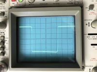
Circuit board with output from drivers is good but when outputs are connected, one pair or 2, no difference, I'm getting some strange ringing. Scope photos below. No load on output. Any ideas? VAS zobel is 100 pF / 100 Ω, Cm is 56 pf in series with 56 pF, 1 kΩ to output rail (TMC).
Photos are upside down, even after rotating and reloading.
1 - 10 kHz square wave, 25 V peak. Positive side looks good, negative side has ringing.
2 - 10 kHz but signal reduced. Note the glitch on the negative swing. Raising signal level causes this glitch to move down and eventually become the ringing.
3 - 2 kHz square wave looks good.
Attachments


Hi steveu,
I have used electrolytic and film capacitors to decouple the power supply on the PCB.
There are always compromises, but given that the simulation does not accurately predict the oscillation - i seem to have the opposite to yourself, simulation runs ok, circuit does not - then i am not sure the dual transistor VAS is as bad as it may seem.
Regards,
Shadders.
My decoupling for both rails is as follows:
Separate wires from the rail fuse to the output transistors and circuit board. At the circuit board, 0.1 µF, 100 µF, diode (to prevent local caps from backfeeding the output during voltage sag), 2.2 Ω, 470 µF, driver collectors (EF2, no predrivers), 22 Ω, 0.1 µF, 100 µF, IPS, VAS, etc., then one more 0.1 µF.
I was able to solve the oscillation problem. The Miller cap is 56 pF, 1 kΩ to output rail, 56 pF. I added 15 pF from one end to the other.
220 pF lag compensation or raising the VAS zobel from 100 pF to 220 pF had no effect. The thing that was / is puzzling me is that the oscillation on the overshoot was only on the negative side. I'm used to seeing symmetric overshoot and oscillation.
Attachments
Last edited:
Hi Fred,Circuit board with output from drivers is good but when outputs are connected, one pair or 2, no difference, I'm getting some strange ringing. Scope photos below. No load on output. Any ideas? VAS zobel is 100 pF / 100 Ω, Cm is 56 pf in series with 56 pF, 1 kΩ to output rail (TMC).
Photos are upside down, even after rotating and reloading.
1 - 10 kHz square wave, 25 V peak. Positive side looks good, negative side has ringing.
2 - 10 kHz but signal reduced. Note the glitch on the negative swing. Raising signal level causes this glitch to move down and eventually become the ringing.
3 - 2 kHz square wave looks good.
Not sure of your design, but if it is not a balanced VAS, then the VAS output may have difficulty switching to a near full on or nearly fully off, depending on how you look at it. Could this be the issue you are seeing ?
Regards,
Shadders.
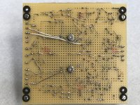
I've never seen so many 0ohm resistors! Do you not want to post the schematic?
Schematic is pencil and paper and needs some cosmetic work before I can scan and post. It's still being marked up with revisions. However, it is very close to that on page 88 of Bobs book except resistors are mostly 1% standard values, no D3-D6, no Q5, C9 is split (TMC), and bias spreader is slightly different. On page 92, I don't have C27. H'mmm. Never noticed that before. Might be something to test.
I also have an offset trimmer injecting at the top of the feedback capacitor, even though IPS and current mirror are beta matched.
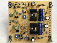
The 0 Ω resistors are to get from here to there and are easier to deal with than cutting jumper wires. Picture of the back side attached. There were still a couple of wires, needed to get to the bias spreader from the board edge. The standoffs are for mounting the other channel above. Trim pots are offset so the right channel trimmers can be accessed through holes in the left channel board.
Attachments
Hi Fred,
Not sure of your design, but if it is not a balanced VAS, then the VAS output may have difficulty switching to a near full on or nearly fully off, depending on how you look at it. Could this be the issue you are seeing ?
Regards,
Shadders.
Quite possible. The problem would be where the VAS turns on heavily (negative slope of the signal). VAS standing current is measured as 10.9 mA at the current source and 11.1 mA at the main VAS transistor. Not sure why the difference, maybe resistor tolerance. I'd think that they should be the same. This is probably affecting output offset, though my power supply rails are also different by 1/2 volt or so. This is an update for a vintage receiver, so there are other loads on the supply that are not entirely balanced.
Schematic is pencil and paper and needs some cosmetic work before I can scan and post. It's still being marked up with revisions. However, it is very close to that on page 88 of Bobs book except resistors are mostly 1% standard values, no D3-D6, no Q5, C9 is split (TMC), and bias spreader is slightly different. On page 92, I don't have C27. H'mmm. Never noticed that before. Might be something to test.
I also have an offset trimmer injecting at the top of the feedback capacitor, even though IPS and current mirror are beta matched.
The 0 Ω resistors are to get from here to there and are easier to deal with than cutting jumper wires. Picture of the back side attached. There were still a couple of wires, needed to get to the bias spreader from the board edge. The standoffs are for mounting the other channel above. Trim pots are offset so the right channel trimmers can be accessed through holes in the left channel board.
Hi Fred,
I'll look forward to seeing the schematic when you are ready to post it. Seeing the full schematic can greatly help us better understand some of the issues you are facing, and revisions that may make the design more stable.
I like the idea of using the 0-ohm resistors as jumpers when their spread is long enough. Packages of jumpers of various sizes and colors are available, and I use them. However, in the kits I've gotten, a color seems to correlate with a size, and I often like to use a color that is somewhat consistent with the function of the wire in the jumper, especially if the jumper is power or ground.
It looks like you are using single-turn trim pots. Although single turn is adequate for some trim functions, I always default to 10-turn pots. This is especially the case for the output stage bias pot.
Cheers,
Bob
- Home
- Amplifiers
- Solid State
- Bob Cordell's Power amplifier book