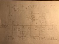
By popular demand, here is a poor copy of the schematic. This is strange. Photos come out upside down. If I make a copy, then rotate so it's upside down, it still comes out upside down. But, if I save and rotate again, it will post correctly. If I simply make a copy and post, it's still upside down.
The driver emitter resistors are 21.5 Ω and final measurement was just under 30 mA. No speedup capacitor.
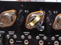
The 2 transistors in the bias spreader are mounted on one driver and one output. As stated earlier, this has been a very good setup. While the drivers maintain constant temperature, there is a major change during initial warmup. Photo of the output sensor. The KSC2690 is completely insulated so it can be clamped directly to the TO-3 case with a custom cut brass strip.
When building, note that transistor pinouts are marked in several places. This is important. All of these are ECB but there are other combinations and I have been guilty of miswiring.
Knight Kit also used precut wires color coded according to length (red = 2", green = 5", etc.) Heathkit had proper colors and you cut to length and stripped.
The single turn pots have not been a problem. I can dial in offset to less than 1 mV but the drift over time is greater than that. Bias is a bit of a compromise as the readings across the 4 emitter resistors do not match anyway. My emitter resistors are (3) 1 Ω in parallel. Crossover distortion can be checked by 1 watt into 4 Ω at 10 kHz. The bias has a huge range with no visible crossover notch. A photo shows that on a lesser amplifier that I was working with a while back. The notch will disappear when the bias is turned up.
The driver emitter resistors are 21.5 Ω and final measurement was just under 30 mA. No speedup capacitor.
The 2 transistors in the bias spreader are mounted on one driver and one output. As stated earlier, this has been a very good setup. While the drivers maintain constant temperature, there is a major change during initial warmup. Photo of the output sensor. The KSC2690 is completely insulated so it can be clamped directly to the TO-3 case with a custom cut brass strip.
When building, note that transistor pinouts are marked in several places. This is important. All of these are ECB but there are other combinations and I have been guilty of miswiring.
Knight Kit also used precut wires color coded according to length (red = 2", green = 5", etc.) Heathkit had proper colors and you cut to length and stripped.
The single turn pots have not been a problem. I can dial in offset to less than 1 mV but the drift over time is greater than that. Bias is a bit of a compromise as the readings across the 4 emitter resistors do not match anyway. My emitter resistors are (3) 1 Ω in parallel. Crossover distortion can be checked by 1 watt into 4 Ω at 10 kHz. The bias has a huge range with no visible crossover notch. A photo shows that on a lesser amplifier that I was working with a while back. The notch will disappear when the bias is turned up.
Attachments

Hi Fred,
Bias current is never a constant, so don't worry about it. DC offset will drift if there isn't a servo, but that should only amount to 20 mV or less from your set value. Some amplifiers with matched diff pairs will be less than 5 mV without any adjustment control and stay there. So I wouldn't worry that much about some drift from your set points.
My rule of thumb is that any amount of DC offset isn't important as long as it is below 50 mV. Some circuits actually have a much higher DC offset designed in, you can't really fix that without seriously mis-matching the diff pair (don't do that), or modifying the circuit slightly (I have been known to do that).
-Chris
Hi Fred,The driver emitter resistors are 21.5 Ω and final measurement was just under 30 mA. No speedup capacitor.
When you refer to the driver emitter resistors, is this the resistor between the two output stage transistors ? The diagram seems to indicate something a lot less than 21.5ohms.
Regards,
Shadders.
By popular demand, here is a poor copy of the schematic.
Looking at this your TMC capacitor values might need to be increased.
A point that may have been escaped notice is the inclusion of a 100R resistor in the collector of the buffer stage (within the VAS) has a collector-to- base capacitance hidden in the diffusion.
The value for such varies under drive - this inversely proportionate (roughly to the the square root) of the voltage applied to the collector.
This part of the stage will have an element of non-linearity and you don't want to amplify any such effects in the VAS second stage.
You could avoid this trouble by eliminating the buffer transistor collector load. As I see it you need to establish your dominant pole for stability via your TMC component values which excludes the use of the 15 pF capacitor.
getting back to the new book
Just received my copy of the new book.
Before I give my copy of the old book away.
Is there anything useful in the old book, that not in the new book?
Just received my copy of the new book.
Before I give my copy of the old book away.
Is there anything useful in the old book, that not in the new book?
Hi Fred,
When you refer to the driver emitter resistors, is this the resistor between the two output stage transistors ? The diagram seems to indicate something a lot less than 21.5ohms.
Regards,
Shadders.
Those resistors are the ones marked as 19.6 on the drawing with a test point between them. They ended up at 21.5 Ω.
Looking at this your TMC capacitor values might need to be increased.
A point that may have been escaped notice is the inclusion of a 100R resistor in the collector of the buffer stage (within the VAS) has a collector-to- base capacitance hidden in the diffusion.
The value for such varies under drive - this inversely proportionate (roughly to the the square root) of the voltage applied to the collector.
This part of the stage will have an element of non-linearity and you don't want to amplify any such effects in the VAS second stage.
You could avoid this trouble by eliminating the buffer transistor collector load. As I see it you need to establish your dominant pole for stability via your TMC component values which excludes the use of the 15 pF capacitor.
An earlier iteration of this did not have the 100 Ω collector load. Bob added that but I don't see an explanation as to why. I have it returned to the signal ground rather than the main ground, but don't know if that makes a difference. The 47 (46.4) Ω resistor is explained.
As for the 15 pF, the "proper" solution would be to increase the 56 pF capacitors but the value would be 86 pF. This could go to 100 pF but I was attempting to keep it as low as possible to keep rise time as fast as possible. Not the most elegant solution, but it does seem to work. 56 pF x 2 worked on the external breadboard but not in the assembled unit. The 15 pF was a later addition. Increasing the second 56 pF to something much larger, often done with TMC, made no difference. Same for the 1 kΩ TMC resistor. But, I can only look at a scope. I don't have a distortion analyzer.
Last edited:
It seems to me like the ringing on the upper square wave edge is due to the VAS turning almost off and the phase penalty that brings. The beta-enhancer especially may cause weird symptoms when it is overloaded.
You have about 1V across 2.15k to bias the beta-enhancer, which equates to about 500uA. I suspect this is not enough to keep this transistor within it's nominal range during the rising square wave edge.
You have about 1V across 2.15k to bias the beta-enhancer, which equates to about 500uA. I suspect this is not enough to keep this transistor within it's nominal range during the rising square wave edge.
It seems to me like the ringing on the upper square wave edge is due to the VAS turning almost off and the phase penalty that brings. The beta-enhancer especially may cause weird symptoms when it is overloaded.
You have about 1V across 2.15k to bias the beta-enhancer, which equates to about 500uA. I suspect this is not enough to keep this transistor within it's nominal range during the rising square wave edge.
That essentially agrees with Bobs numbers (500 µA), so let's see what he has to say on this. The comments have been interesting.
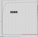
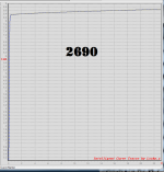
Also if Bob used the KSC3503 and you use the KSC2690, it could be that your transistor is just harder to drive (I don't have datasheets memorized, but I think the KSC2690 is slower). The KSC3503 is hard to beat. So maybe in bob's design it was a non-issue. Just shooting from the hip.
That essentially agrees with Bobs numbers (500 µA), so let's see what he has to say on this. The comments have been interesting.
Just look at the collector current waveform of that transistor during the square wave edges in simulation. I think the question is whether during positive slew rate limiting does the resulting current through the collector-base capacitance of the VAS transistor exceed 500 uA. If slew rate is 50 V/us and Ccb is 5 pF, I is 50e6 * 5e-12 = 250 uA if I have not made a mistake. Just throwing out some numbers here. Bear in mind that Ccb varies with Vcb, and it can get fairly small as the voltage at the collector of the VAS transistor rises.
Cheers,
Bob
Also if Bob used the KSC3503 and you use the KSC2690, it could be that your transistor is just harder to drive (I don't have datasheets memorized, but I think the KSC2690 is slower). The KSC3503 is hard to beat. So maybe in bob's design it was a non-issue. Just shooting from the hip.
fT is essentially the same. However, Cob is 2.6 pF (3503) vs. 19 pF (2690) which is a large difference.
An earlier iteration of this did not have the 100 Ω collector load. Bob added that but I don't see an explanation as to why. I have it returned to the signal ground rather than the main ground, but don't know if that makes a difference. The 47 (46.4) Ω resistor is explained.
As for the 15 pF, the "proper" solution would be to increase the 56 pF capacitors but the value would be 86 pF. This could go to 100 pF but I was attempting to keep it as low as possible to keep rise time as fast as possible. Not the most elegant solution, but it does seem to work. 56 pF x 2 worked on the external breadboard but not in the assembled unit. The 15 pF was a later addition. Increasing the second 56 pF to something much larger, often done with TMC, made no difference. Same for the 1 kΩ TMC resistor. But, I can only look at a scope. I don't have a distortion analyzer.
The 1k value should be left alone.
The breadboard circuit did not include the output transistors doing so changes the rules of the game since these are slower than the driver transistors and also the load on the VAS collector transistor is increased reducing the loop gain.
You just have to accept in terms of your ceiling frequency that this is going to be lower and if you shoot to exceed this the EF2 stage will fall off the pace.
Apart from your EF2 output stage loading on your VAS transistor you have covered a number of bases for your compensation - TMC, Miller, and lag (your zobel).
The dominant pole has to be 10 times more effective in reducing frequency response than any other. You don't want to create rival poles to upset the balance of power.
You have your primary TMC network which should be sufficient if executed with the right value capacitors. Alternatively you could also try a single Miller capacitor.
In any case your capacitors should be NP0 dielectric types. Looking at the photo of your board I have doubts about this. As to values you will have to do this hands on by old fashioned trial and error.
If you are intent on TMC rather than Miller compensation the shorter route could be to start with a high value like 220 pF and see where this leads.
The breadboard did include a single pair of outputs but the emitter resistors were the rectangular sand type and may be wirewound.
The ceramic caps are NP0, Digi-Key 399-14032-ND and 1012PHCT-ND. I have used 220 pF but lowering the value as much as possible before the ringing starts does help rise and fall time. The VAS zobel was the major improvement. C is 100 pF, not 220. Diagram shows both numbers but increasing to 220 pF made no visible difference. As stated earlier, this is now mostly hands on experimentation. I'm ok with the result at present but if there were obvious improvements, I'd consider changes.
Again, no distortion analyzer. I did listen to music using the breadboard driving 4 speakers, series/parallel, for an 8 Ω load and did not notice any problems.
As for EF2 vs. EF3, 50 watts into 4 ohms is 5 A peak. This is divided between 2 output transistors at 2.5 A each. Beta droop is very small at that point and beta is between 50 and 60. That was measured using a circuit that pushed about 2 A through the devices as opposed to microamps from a typical transistor tester. Drivers are better than 150, so VAS loading for this calculates to 0.67 mA peak with a 10 mA standing current. The power supply is probably not capable of that much power at 4 Ω, though I'm trying to get to 50 W at 8 Ω, limited to the existing transformer.
I'll scope the VAS driver and drive it into clipping and have a look.
Thanks for the input.
Last edited:
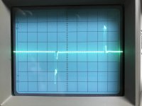
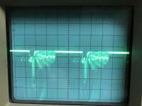
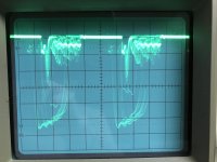
Scope traces from the VAS driver collector. All are 10 kHz square wave.
1 - 4 V out, 2 mV spikes
2 - 25 V out (safely below clipping), 50 mV spikes
3 - Hard clipping, spikes are 100 mV per division. I think the 0 V line is centered.
4 - Same but baseline moved up to show the bottom part of the spikes
1 - 4 V out, 2 mV spikes
2 - 25 V out (safely below clipping), 50 mV spikes
3 - Hard clipping, spikes are 100 mV per division. I think the 0 V line is centered.
4 - Same but baseline moved up to show the bottom part of the spikes
Attachments

Last edited:
Scope traces from the VAS driver collector. All are 10 kHz square wave.
1 - 4 V out, 2 mV spikes
2 - 25 V out (safely below clipping), 50 mV spikes
3 - Hard clipping, spikes are 100 mV per division. I think the 0 V line is centered.
4 - Same but baseline moved up to show the bottom part of the spikes
I refer the transistors in your CCS for the LTP and VAS stages in your circuit.
In the voltage reference transistors in each there is high resistance via the emitter to base junction passing current to earth.
The restriction of current is going to affect the base emitter junction voltage drop
Normally there would be no base stopper resistor in which case the voltage drop between emitter and base will be larger than in your circuit around the order of 0.6V.
This is a compromise you could do without I such also that you take an extra step of making the two CCS structures independent with each having it's own separate resistor to earth.
This will change some working voltages elsewhere. It should be possible to achieve an accurate level of dc offset without the addition network you have included for that purpose.
A small de-coupling cap on the VAS driver collector can be useful, but of course if the cap is too large then we have clipping problems again. And the collector resistor can be a divider to reduce the collector voltage so that a fast low voltage transistor can be used.
Hi All.
Just wondering if somebody can explain to me how the value of 200K was caculated for the input impedance to the Darlington VAS shown at the bottom of page 68 of bob 2nd edition.
Thanks.
Just wondering if somebody can explain to me how the value of 200K was caculated for the input impedance to the Darlington VAS shown at the bottom of page 68 of bob 2nd edition.
Thanks.
Last edited:
Bob
I have +/- 65 volt rails ( and +/-75V for the driver board). Which output device would I be better to use for a 250 watt/8 ohm power amp? 4 of Hitachi 2SJ56/2SK176 or 4 of Toshiba 2SJ201/2SK1530. The Borbely FET driver board will accommodate either. I have enough devices to make up matched quads of either type. The load is electrostatics.
I have +/- 65 volt rails ( and +/-75V for the driver board). Which output device would I be better to use for a 250 watt/8 ohm power amp? 4 of Hitachi 2SJ56/2SK176 or 4 of Toshiba 2SJ201/2SK1530. The Borbely FET driver board will accommodate either. I have enough devices to make up matched quads of either type. The load is electrostatics.
Last edited:
- Home
- Amplifiers
- Solid State
- Bob Cordell's Power amplifier book