I like your boards - very smart 🙂
Do you use a special jig to bend the legs of your transistors (to get the bend in the correct place every time)?
no special jig, just drill bit
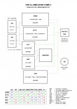
excuse me for little promotion, the family 😀
Attachments
Yes because most of the amps in selfs book are 2 EF so none of them designs that he ever did are really good obviously and never have good slam sound and even with 6-8 parallel pairs all of those 16A will be going through just one pair of course and this is super big beta droop territory at 16A bro! What about (you don't mention) a 2 EF output stage with minim current gains of 5 and 2 in the drivers and output transistors? You have a current gain of 10 (if my maths right) and super nonlinear now and need 1.6A peak from the vas to drive it! WOW!!!!!!!!!!!!!! vas will die transistors and 2 EF sux totally unusable in any respectable design.
I do seem to recall Self saying on a thread here somewhere that he has not put into production an amplifier with a triple output stage. I could be wrong, but that is what I recall. My belief is that one cannot really attain truly good amplifier performance without a triple output stage of some sort. The last time I built a 2 EF output stage was in 1970 when I cloned a Citation 12.
Bear in mind, there are many, many ways to implement a triple output stage, only one of which is the 3 EF Locanthi stage. Another good one is the diamond buffer triple (DBT), wherein the EF output stage is preceded by a diamond buffer. Still another is an EF output stage preceded by a CFP. One can even just preceded a 2 EF output stage with a single-ended EF between the VAS and the output stage.
Triples can sometimes be more difficult to stabilize, but that is no reason to not use them. If you always use progressive power supply bypassing (series R, shunt C) as the rail progresses from the output transistors back to the drivers and then pre-drivers, that will be a big step in aiding stability. The low impedance of the R-C rail networks can also act as a Zobel network on the rails, damping any tendency to resonance. If you center-tap the driver emitter resistor in a Locanthi Triple and connect the center tap to ground through a 2200 pf capacitor (for example), that will form a Zobel network that will also promote stability.
Always make sure that the usual output Zobel network is physically close to the output rail and output transistors, and that the power transistor rails are bypassed at high frequencies to pretty much the same ground as the Zobel uses. Use of multiple output Zobel networks in parallel, each using 2 or 3-watt metal oxide film resistors, is also helpful. If using multiple such Zobels, put them at different places on the output bus. Inductance in the output stage, especially when it is not damped, is not your friend.
Cheers,
Bob
I do seem to recall you stating that examples of your Vertical MOSFET amplifier, minus the HEC and without TMC/TPC, achieve typical THD-20kHz figures of around 0.02%.I do seem to recall Self saying on a thread here somewhere that he has not put into production an amplifier with a triple output stage. I could be wrong, but that is what I recall. My belief is that one cannot really attain truly good amplifier performance without a triple output stage of some sort. The last time I built a 2 EF output stage was in 1970 when I cloned a Citation 12.
Bob
Most of Self's 2EF plain vanilla Miller-compensated amplifiers better that quite easily, but your pretensions are noted.
But I guess we can just be completely arbitrary about what we call "truly good amplifier performance". And your suggested minimum driver and output transistor gain figures of 50 and 20 respectively, from your previous post, as you well know, are overly pessimistic.
I notice that some of John Curl's power amp designs for Parasound, have an output stage which is a "Double" not a "Triple". HOWEVER the driver is built with MOSFET source followers instead of BJT emitter followers. Shazam! The current gain of this output stage equals (Infinity * Beta). That's a very big number.
For example here is the Parasound HCA-1200 power amp. Beware, their schematic symbols are a little goofy and nonstandard, but you can verify that Q115 = 2SK1529 is a MOSFET {datasheet below} and Q121 = 2SJ200 is also a MOSFET {datasheet below}.
It may be useful to analyze the Parasoud output stage a little differently than Bob's book analyzes an all-BJT output stage. Instead of assuming that its input impedance = (Zspeaker * CurrentGainOfOutputStage), it might prove to be more useful to assume that its input impedance = (100% of CGD + 1% of CGS) of the MOSFET. Since the almost-unity-gain of the MOSFET source follower, bootstraps away almost all of CGS.
_
Attachments
I used an EF2 in my nx-Amp (100 watts per channel) and get about 0.02% distortion.
I’ve used EF3’s (‘Locanthi T’ configuration) on all of my other designs without problems and getting about 15x lower distortion. Importantly, with an EF3, the distortion remains low even with low speaker impedances, which an EF2 cannot match and that to me is the big benefit.
The advice in your book about EF3 OPS decoupling etc is invaluable - very important that trace inductances, loop areas, rail decoupling and base stoppers are applied rigorously if a good result is to be had.
Hi Bob and others, Happy New Year as well.
I always enjoy reading what you have to say about audio amplifier design.
As you know, the pcb design is an integral part of the complete design, it can make or break your wonderfully simulated design.
My offer still stands, that I will do a power amp pcb layout for you and the readers. I might be able to get it done in time for your new book revision release. Maybe you have done this already and do not need my assistance, that is great, but if not, let me know if you are interested in my offer. I certainly would like to design a pcb just for you, just the way you would like it done as if I was working for you.
Thanks and cheers
Rick
Last edited:
I notice that some of John Curl's power amp designs for Parasound, have an output stage which is a "Double" not a "Triple". HOWEVER the driver is built with MOSFET source followers instead of BJT emitter followers. Shazam! The current gain of this output stage equals (Infinity * Beta). That's a very big number.
For example here is the Parasound HCA-1200 power amp. Beware, their schematic symbols are a little goofy and nonstandard, but you can verify that Q115 = 2SK1529 is a MOSFET {datasheet below} and Q121 = 2SJ200 is also a MOSFET {datasheet below}.
It may be useful to analyze the Parasoud output stage a little differently than Bob's book analyzes an all-BJT output stage. Instead of assuming that its input impedance = (Zspeaker * CurrentGainOfOutputStage), it might prove to be more useful to assume that its input impedance = (100% of CGD + 1% of CGS) of the MOSFET. Since the almost-unity-gain of the MOSFET source follower, bootstraps away almost all of CGS.
_
Exactly right, Mark. Using a MOSFET as a driver pretty much eliminates the need for a three-stage output stage. You are also correct in pointing out that the Cgd of the MOSFET driver is the main thing in play there, and to look out for.
It is also worth pointing out that safe operating area of the drivers, especially in big amplifiers, must also be adequate. MOSFETs as drivers can help in this way as well.
Speaking of capacitance to be driven by the VAS, and returning to all-BJT output stages, if we choose BJT drivers with enough SOA to drive a good-sized output stage, the Ccb of the drivers might be a little more than we would like for loading the VAS. Here we have another good case for a triple, where we can use a smaller pre-driver transistor, often of the same type of device as the VAS.
Cheers,
Bob
I think he has given up on my offer as well 🙂
Please do not take this the wrong way but ...
I just find it odd that someone could write a book of this type having 100's of pages of design information. Not one actual working example demonstrating the complete design process, so that it can be shared and built by the DIY community, that they can be entertained and enjoy the fruits of their labour.
Am I missing something here? Maybe many who buy the book have the resources & inclination to design their own pcb's & power amps without fail or is it just meant as reading material with no physical application by the majority of readers. Theory without actual hands on practice and working examples. In that case, the book falls short on physical working results.
Hi Rick,
To the contrary, the second edition contains an entire chapter covering an example amplifier from soup to nuts, including detailed coverage of testing and troubleshooting. This is just what I also felt needed to be added to the book. It is not the only design that has been built and measured. It is one of numerous different ones that were built and measured, not just simple variations on one basic design.
Your kind words and offer in your earlier post are deeply appreciated, and we should talk. Writing a book of this size, depth and breadth is a very difficult undertaking, and I have not been able to do all that I would like to do, even given the much longer time it has taken to write the second edition than I had hoped or expected. A great deal of time and research went into some new topics, like switching power supplies, which is now the longest chapter in the book. Page count limits have also played a big role in constraining both editions. Attempting to simultaneously meet the needs of the enthusiast, professional and educational communities is also a challenging balancing act.
To answer Jack's question, I have not given up on ThermalTrak transistors, and in fact have included the details on the ThermalTrak amplifier that I built and measured for the first edition.
Cheers,
Bob
My mistake. Cordell used Hawksford Error correction in his error correction circuit.
Has anyone bookmarked some of the attempts others have made at improving it?
My attempt:
Error-correction power amp | Linear Audio NL and here are the individual articles:
https://linearaudio.nl/sites/linearaudio.net/files/UK-1 2008040241.pdf
https://linearaudio.nl/sites/linearaudio.net/files/UK-2 2008050441.pdf
Jan
Hi Bob,
"From soup to nuts", does that include a complete pcb assembly (pcb fab data, BOM, assembly/test documentation) that the readers can build themselves? If so, you have accomplished what I deem a missing link in having at least one working example of your book contents.
I understand completely the time and effort involved to get the second revision out. I commend you, in this endeavour. This is why I have made my offer to help you if it fits your needs. So "Lets talk", by all means, I am genuine in helping you out and work with you.
Sincerely
Rick
Hi Rick,
The book has numerous measured working examples of amplifiers implemented with different topologies and technologies. However, the example in the new chapter that I referred to as a soup-to-nuts description is not a complete construction project as might appear in a magazine. Rather, it is a complete amplifier that includes all aspects of the design as a fully working system, including things like power supply and comprehensive protection circuits. It is a complete design that someone can build. Its intended as a good getting-started project.
Every aspect of the amplifier is thoroughly described and the amplifier is fully measured. All of the steps from initial testing in planned steps to troubleshooting are covered in detail. At the end of the chapter, optional design enhancements are discussed.
The amplifier is one of the designs described in the preceding "amplifier evolution" chapter taken to the real world. A big part of the intention is to allow those readers who choose to build an amplifier before reading the whole book to do so. It is a well-performing "getting started" design that is straightforward and complete. It is not a pretentious design. It is a straight Miller-compensated all-bipolar design with a two-pair output triple. Depending on power supply, it will do up to about 150W into 8 ohms.
However, the amplifier is not a complete "construction project" in that it does not include a PCB design and fab data. The design is presented as being on 3 boards, the main one containing the IPS, VAS, bias spreader and pre-drivers. A second board contains the output stage and a third board implements the protection circuits.
Send me a PM with your email and we can talk further. I appreciate your interest in this project.
Cheers,
Bob
Hi,
Book should be due 15th May 2019. Hurrah.
Designing Audio Power Amplifiers: 2nd Edition (Paperback) - Routledge
Regards,
Shadders.
Book should be due 15th May 2019. Hurrah.
Designing Audio Power Amplifiers: 2nd Edition (Paperback) - Routledge
Regards,
Shadders.
Hi Bob,
I think the sample design is excellent idea and very helpful. Despite running many simulations, there is always a vast amount of anxiety as to whether the design will work. Same for the protection circuits too.
I took the figure 3.14 in the current book, used a pair of transistors for the output and a triple, cascode VAS, parallel input transistors for the LTP, and achieved 0.007% THD for 20kHz, peak 500watts into 4ohms. Again, still trepidation before commiting to PCB fabrication.
Regards,
Shadders.
Congratulation! Sounds like you did a great job!
You are right about simulation. There is nothing like the real thing on the bench. SPICE helps us to get to where we want to be with less time wasted.
As you know, I am a strong advocate of simulation for many reasons. First it is a great tool for checking for dumb mistakes; second, it is a good tool for comparing different circuits to see relative differences in performance; third, it is a great tool for refining a design and understanding tradeoffs. Fourth, it can give you some indication of what performance to expect. Its ability to easily probe voltages and currents anywhere in a circuit can be extremely helpful.
SPICE will not always be highly accurate for absolute performance for many reasons, including imperfect and incomplete models and the fact that real-world parasitics are usually not well modeled, if at all, but it can certainly point you in the right direction. I will virtually never build a circuit without simulating it in SPICE first.
It is also a great teaching tool. In particular, it can show how things should work, without the results being clouded by parasitics and other effects in the real world. Sometimes we'll see some effects on the lab bench that we do not understand, or which are non-intuitive, and we may resort to speculating on what the cause is. Doing some SPICE runs can often help us test out some of those hypotheses.
Cheers,
Bob
Dear Bob, I've read your book and I find it very interesting and informative, I have, however, one question which perhaps has already been answered in this huge thread.
Why do you use degeneration resistors in the emmiter of the VAS?, in Douglas Self's book, he says that there is no need for degeneration resistors in the VAS since the input of the VAS is a current rather than a voltage, so the voltage at the base of the VAS transistor is very small (thus the signal voltage of the emmiter is also very small). Douglas Self essentially considers the VAS as input current in-output voltage out, whilst you seem to consider it a voltage in-voltage out
Why do you use degeneration resistors in the emmiter of the VAS?, in Douglas Self's book, he says that there is no need for degeneration resistors in the VAS since the input of the VAS is a current rather than a voltage, so the voltage at the base of the VAS transistor is very small (thus the signal voltage of the emmiter is also very small). Douglas Self essentially considers the VAS as input current in-output voltage out, whilst you seem to consider it a voltage in-voltage out
These are good questions. Interestingly, in Self's 6th edition there is almost no amplifier that does not have emitter degeneration in the VAS. Indeed, if for no other reason, you need an emitter resistor to sense current for the conventional way of implementing current limiting in the VAS.
The VAS can be viewed in many different ways, especially depending on the frequency range when you include the Miller compensation capacitor as part of what you are calling the VAS. At very low frequencies, usually below the open-loop bandwidth, the VAS tends to act as voltage in, voltage out, assuming that the IPS is loaded resistively in some way and that the impedance at the VAS collector has some reasonably finite value, such as the output impedances of the VAS transistor and current source and input impedance of the output stage, all in parallel.
However, in a Miller-compensated VAS, the VAS acts more like a transimpedance stage as a result of the shunt feedback of the Miller capacitor. In this case, it is largely current in, voltage out. However, if you do not consider the Miller compensation capacitor as part of the VAS, then the VAS is more like a voltage in, voltage out stage with shunt feedback around it. Also, if you are using shunt lag compensation instead of Miller compensation (not generally recommended), then the VAS acts more like a voltage in, voltage out stage.
No matter how you choose to look at it, I always believe in having each stage of the amplifier be as linear as possible, and emitter degeneration of the VAS helps that by providing some local feedback in addition to the shunt feedback provided by the Miller capacitor. Also, emitter degeneration increases the output impedance of the VAS transistor and decreases the influence of the Early effect. A 2 EF VAS with emitter degeneration can have a quite high output impedance, even without resorting to a cascode. I always use emitter degeneration in the VAS, even though there will likely be those who assert that it is not necessary or helpful.
It may not be strictly "necessary", but almost everyone ends up using it.
Cheers,
Bob
Thank you Bob, that was really helpful. BTW theres an amazon pre-order sale of your 2nd edition book which according to Amazon will be released on May, is this correct?
Last edited by a moderator:
Thank you Bob, that was really helpful. BTW theres an amazon pre-order sale of your 2nd edition book which according to Amazon will be released on May, is this correct?
Yes, the second edition of Designing Audio Power Amplifiers is available for pre-order on Amazon and will be available on May 17.
The book is 776 pages, with 36 chapters (5 new chapters). Many of the chapters from the first edition have been updated and/or expanded.
The new chapters include:
- "Building an Amplifier" (a very detailed example)
- "Noise" (an in depth treatment of noise theory and practice)
- "Output Stages II" (much additional information on output stages)
- "Switching Power Supplies" (the SMPS chapter is now the largest chapter)
- "Professional Power Amplifiers" (coverage of special needs and features)
The table of contents is available on the Routledge site at the following link:
Designing Audio Power Amplifiers: 2nd Edition (Paperback) - Routledge
Cheers,
Bob
- Home
- Amplifiers
- Solid State
- Bob Cordell's Power amplifier book