Hi Ar2,
that PSU you PDFed.
The two banks of caps, the first stage before the 0r22 and second stage after the 0r22 share a common return for the 0v.
Most of the short duration charging pulses are absorbed by the first cap bank.
The charging pulses after the 0r22 are very attenuated (it is much closer to DC).
The second bank will suffer from the voltage modulation on the 0v connection back to the transformer centre tap and the leg down to the central ground.
I think it would help to break the 0v connection between the two cap banks and run a separate 0v lead from the second bank to the central ground.
What do you think?
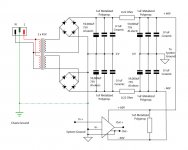
Here I made some changes in the drawing so it is more clear.
Andrew is this ground plan - 0V what you had on your mind?
I haven't seen that kind of broken ground between caps, but what are you saying is making sense.
AR2
Edit: Now that I am looking into the schematic, I think we need to clarify the terminology: There is chasis ground - connected to earth ground from the AC plug, and there is system ground - 0V. When you say central ground what are you reffereing to? I draw dotted green line between chasis ground and system ground as those two do not need to be connected. If they are not than system ground is ( I am assuming you are reffering to) central ground. Than in that case I do not understand breaking the 0V line between the two banks of caps. Please advise.
Attachments
Hi Ar2,
you understood it correctly,
Now test it and tell us if you agree?
That broken green line is the disconnecting network.
It's ONLY purpose is to make the amplifier safe to operate.
The system ground = audio ground = central star ground and it should float separate from the safety earth.
ALL ground connections that are audio related should be isolated from the chassis.
I do agree with everything you mentioned regarding chasis and system ground. My question was regarding broken 0V line between two banks of caps. Let say I install star ground on the top of second banks of caps (screw mount caps, and I will make thick coper board on the top) The distance between two cap banks is 3" (they are each 3" in diameter and they are touching each other) Since both banks are connected to star point of system ground (on the top of the second bank) than first bank of caps is just like before we dissconected the 0V line. In another word, if I understood you correctly, the difference between broken 0V line and unbroken line is only few inches and they both need to connect to the same point. Does that make any difference?
Hi,
I have always tried to dissuade builders from putting the audio star ground on the common plate between the smoothing caps.
The worst pulse currents are confined to the first set of caps and to the connection to the centre tap.
The much smaller pulsing currents between the second bank of caps is less of a problem but still significant.
Take an example.
2Apk charging current through a 1mohm connecting wire will generate a 2000uV modulation across that wire. If you substitute a copper plate and reduce the resistance to 100uohms then that same 2A will cause 200uV of modulation across the plate. If this modulation were allowed to appear across the input ground of your amp then that would produce a voltage at the output that is only -74db below maximum output of a 100W amplifier.
You should be striving for better than -120db. To get that -120db, the modulation on the input ground must be below 1uV. One must think how to cancel out the voltages/resistances not just making them smaller.
If the main currents through the second bank are smoothly changing audio signal then the problem is less than the charging pulses but should still not be ignored. The sudden changes from ClassAB rails will be intermediate in their effect.
I have seen a PCB star ground layout that almost works and the logic can be applied here.
Put a set screw through the 0v plate.
On the bottom side attach the centre tap, then the first bank 0v connection and next to the screw head put on the connection to the disconnecting network .
On the top fit a nut.
On top of that nut place your highest current returns, dirtiest first, then add on the low current returns, cleanest last and a final nut.
Sugden used the pcb as their star ground with the copper side (=cap 0v) touching the dirty returns and the insulated side for the clean returns. The screw became a very short connection. This is the only place I have seen this done but I suspect there are many others that have developed a similar cancelling assembly.
Not many adopt RCRC filtering on a power amp PSU and some of them do not appreciate that solid copper connecting wire has resistance. That may be why your layout and my suggestion may seem unfamiliar.
Andrew thank you very much for such a detailed description. What a primer on grounding! I will slowly digest this line by line.
Since you are not recommending using the top of capacitors as a star ground point (unless implemented as described) would you mind describing ideal scenario and position of a star ground.
Thank you
AR2
Since you are not recommending using the top of capacitors as a star ground point (unless implemented as described) would you mind describing ideal scenario and position of a star ground.
Thank you
AR2
there is a practice with electrical wiring wherein it says, "do not rely on the bolt to carry current".
with this in mind therefore, i do my star grounding using ring lugs wherein all the lugs are fixed one on top of each other and then using a flat-washer, spring washer then the nut tightened into the bolt. works great for me....😀
with this in mind therefore, i do my star grounding using ring lugs wherein all the lugs are fixed one on top of each other and then using a flat-washer, spring washer then the nut tightened into the bolt. works great for me....😀
Hi,
If you look back to the earlier suggestion, you will see that some want to group the grounds into dirty, high current, low current and then link them together.
The above (bolted method) meets that criteria, it's just the links are VERY SHORT.
I try to locate the star audio ground central between Transformer, Smoothing and Amplifier. Keep all the wires as short as possible (=keep the layout compact) and where a pair flow and return twist them together (+,-&0v form a twisted triplet).
I just miss out the spring washer. This makes it easy to experiment with alternative grounding and easy dismantling rather than trying to solder all the ends together.i do my star grounding using ring lugs wherein all the lugs are fixed one on top of each other and then using a flat-washer, spring washer then the nut tightened into the bolt.
If you look back to the earlier suggestion, you will see that some want to group the grounds into dirty, high current, low current and then link them together.
The above (bolted method) meets that criteria, it's just the links are VERY SHORT.
I try to locate the star audio ground central between Transformer, Smoothing and Amplifier. Keep all the wires as short as possible (=keep the layout compact) and where a pair flow and return twist them together (+,-&0v form a twisted triplet).
AndrewT said:Hi, I just miss out the spring washer. This makes it easy to experiment with alternative grounding and easy dismantling rather than trying to solder all the ends together.
If you look back to the earlier suggestion, you will see that some want to group the grounds into dirty, high current, low current and then link them together.
The above (bolted method) meets that criteria, it's just the links are VERY SHORT.
I try to locate the star audio ground central between Transformer, Smoothing and Amplifier. Keep all the wires as short as possible (=keep the layout compact) and where a pair flow and return twist them together (+,-&0v form a twisted triplet).
I guess I take a slightly different view. Of course, grounding stuff is very subjective. As I have mentioned before, my preference generally leans to a star-on-star ground topology, where we can intentionally manage where the ground currents are flowing, and where we can segregate high noise currents away from flowing within the single point ground, at least to some extent.
In the diagram that was shown, where the first and second rail capacitors were separated by a 0.22 ohm resistor, I would have made the ground junction of the second two capacitors (the ones on the load side) the central reference ground for the amplifier. The rectifier noise currents flowing through there are much, much lower than the currents flowing at the junction of the first set of capacitors. I would have made that latter ground junction a star off of the main star ground I identified above. Although the wire connecting that satellite star to the main star ground has finite resistance, the key is that any small voltage appearin across that link is of little or no consequence.
Bob
I would also take the two (4) high-Q caps that are in parallel to the first reservoir caps (the ones directly at the left after the rectifier), and instead would place them directly at the load. That is where they have maximum effect.
Jan Didden
Jan Didden
jacco vermeulen said:Mr C,
any chance of a picture of your grounding Universe for 3d grades ?
"Grounding Universe" - that's a cool term for the star-on-star approach! I'll have to give some thought to how best to portray it as a picture. Hmmm... stars rotating around stars?
BTW, I think most of us are unknowingly using star-on-star topologies to begin with; it's just a matter of degree and explicitness. For example, let's say we are going to be fancy with our amplifier and make it a four-layer board that incorporates two internal ground planes, one "signal" and one "power". We return each one of these ground planes separately to the amplifier's star ground. Each of those ground planes has multiple components connected to it. In a sense, each of those ground planes is like a star on the main star (to the extent that the ground plane is equipotential, it can be thought of as a star).
Cheers,
Bob
Cheers,
Bob
I've been calling a similar arrangement a "hierarchical ground"
where the base of the hierarchy is the noisiest connection
(transformer center tap and first PS capacitors) and the apex
is the input signal ground.
😎
where the base of the hierarchy is the noisiest connection
(transformer center tap and first PS capacitors) and the apex
is the input signal ground.
😎
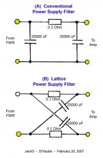
This is in reference to the contributions that discussed the C-R-C pi-network for power supply filtering. Due to the small series resistor of about 0.2 Ohm, the large charging peaks will be mainly absorbed by the first capacitor, whereas the following RC can be viewed as a lowpass filter (sort of).
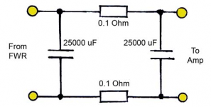
There is an alternative where both capacitors share equally in handling the current peaks. This symmetry is achieved if the circuit is wired as a lattice filter. In the attached figure, both filters have the same dc-voltage loss due to the resistor (which needs to be split for the lattice arrangement). To keep it simple, film bypass caps are not shown in the drawing.
I could imagine that the symmetric use of the caps could actually be a plus, but I have not made any comparisons between the two arrangements in regard to resulting output ripple or sonics. Maybe someone with an implemented pi-network can make a quick rewire and report? This would have to be done on the positve and negative supply, assuming they are fed from separate windings and full wave rectifiers (FWR).
To experiment, one can add additional caps at the input and output of the lattice (the one at the output would be on the amplifier board).
Any thoughts?
Kurt
Attachments
Nixie,
I agree. I showed the top version the way it has been shown in previous posts. Note, that although your redraw has symmetry, it is not equivalent to the lattice wiring.
Kurt
I agree. I showed the top version the way it has been shown in previous posts. Note, that although your redraw has symmetry, it is not equivalent to the lattice wiring.
Kurt
Why are you pointing that out? I never claimed it did!Javin5 said:Note, that although your redraw has symmetry, it is not equivalent to the lattice wiring.
i have always returned the speaker leads to the star ground, transformer, caps and never to the pc boards. i run separate ground wires for them......😀
here is how i do it in sequence, from bottom up:
1. transformer center tap lead
2. filter caps leads
3. speaker return leads.
4. pcb earth lead,
5. input jack earth
here is how i do it in sequence, from bottom up:
1. transformer center tap lead
2. filter caps leads
3. speaker return leads.
4. pcb earth lead,
5. input jack earth
Nixie said:I prefer the version below to that of the top one in your diagram. I find I get cleaner ground that way (circuit is grounded at the right bottom node).
Nixie, in your schematic translated to the dual brudge situation you have resistor in series with 0V - system ground? Wouldn't that be a problem if grounds are at different levels?
- Status
- Not open for further replies.
- Home
- Amplifiers
- Solid State
- Bob Cordell Interview: Power Supplies