Hi,
I prefer the economics of a single big transformer with four secondaries to allow independance of the two channel PSUs.
Each channel would have a dual rectifier to allow independance of the audio grounds. Both audio grounds have their own disconnecting network to the safety earth.
The big transformer gives the benefit of good regulation,
the separate PSUs reduce the crosstalk
AndrewT said:Hi,
I prefer the economics of a single big transformer with four secondaries to allow independance of the two channel PSUs.
Each channel would have a dual rectifier to allow independance of the audio grounds. Both audio grounds have their own disconnecting network to the safety earth.
The big transformer gives the benefit of good regulation,
the separate PSUs reduce the crosstalk
Keeping separate grounds for the left and right channel is an interesting point. Do you think that is the origin of the preference by some for dual-mono approaches?
What is the primary advantage of dual rectifiers over a single bridge with a center-tap, in your opinion? The former drops through twice as many diode drops.
Thanks,
Bob
This was covered before, I believe in this thread. Look for post by Nelson Pass. Use of dual rectifiers prevents the ground current from passing back into the transformer and creating a distorting (DC) flux in the core.
single rectifiers force the centre tap to be common to both channels.Bob Cordell said:Keeping separate grounds for the left and right channel is an interesting point. Do you think that is the origin of the preference by some for dual-mono approaches?
What is the primary advantage of dual rectifiers over a single bridge with a center-tap, in your opinion? The former drops through twice as many diode drops.
I was never able to prevent hum in the output with this cheaper and simpler arrangement of two channel amplifier construction.
Dual rectifiers allows the audio ground for each channel to be completely separate. The cost and voltage loss being the two downsides.
A monoblock does not see any advantage in going to dual rectifiers. Similarly a 4secondary should be able to work with single rectifiers but I have found this more susceptible to small changes in wiring increasing the hum problem.
pooge said:This was covered before, I believe in this thread. Look for post by Nelson Pass. Use of dual rectifiers prevents the ground current from passing back into the transformer and creating a distorting (DC) flux in the core.
This seems to make sense, but then I got to thinking about it. Maybe I'm just having a fuzzy day. Lets say the transformer has two windings, A and B, A on top, B on bottom.
In the dual rectifier case, winding A feeds the bridge for the positive half of the supply and winding B feeds the negative bridge.
In the single-bridge case, the top of winding B is connected to the bottom of winding A, forming the center tap, which is connected to ground. The outer ends of the windings feed the bridge in conventional fashion.
Let's assume we are taking current only from the positive supply output, so there is a current imbalance.
In the dual rectifier case, we have opposite-direction currents on opposite half cycles in winding A only. There is no net dc flux. There is no current in winding A.
In the single-rectifier case, winding A sees a half-wave current on positive half cycles. Winding B sees a half-wave current on negative half cycles. Each winding, looked at by itself, sees a net average DC current. However, because of the winding directions, the net flux as seen by the core is, I think, the same as in the dual rectifier case above, namely zero in the ideal case.
Am I correct? I realize that even if I am correct, this situation might not be desirable in light of slight winding mismatches between windings A and B.
Cheers,
Bob
Am I correct? I realize that even if I am correct, this situation might not be desirable in light of slight winding mismatches between windings A and B.
that is why i wind my traffo secondaries biflliar, thus voltages are exactly the same.....😀
i have never tried dual secondaries feeding two bridges for positive and negative supplies, i don't seem to miss them at all...
i do my grounding in this manner from the groundpoint bolt, order of earthing cables from bottom up:
1. transformer center tap lead.
2. the 2 leads from the main filter caps, pos and negative.
3. the leads from the speaker jack return.
4. earthing cables for main amp pcb.
5 earthing leads from input jacks
i never had to contend with hum problems, dead quiet....😀
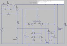
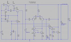
Here is a little shunt regulator I’ve designed to provide the low power +/-75V supply rails for a class A amp I am building. Shown below is the positive half. The negative half will be identical, except the NPN's swapped for their PNP complements and vice versa. Efficiency was not a design concern.
Stability is rendered unconditional by the 470uF output shunt capacitor and PSRR (or ripple rejection) simulates better than 120dB out to 20kHz.
Stability is rendered unconditional by the 470uF output shunt capacitor and PSRR (or ripple rejection) simulates better than 120dB out to 20kHz.
Attachments
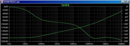
Here is a dynamic load test. The 100mA load (750 ohm resistor) is switched in and out of circuit at a rate of 1kHz. The load/no load level shift is about 400uV, indicating a “DC” output resistance of 4 milli ohms.
The key to this designs performance relies on the fact that the intrinsic output impedance (prior to the application of NFB) of a shunt regulator is very high. This means that an output stunt capacitor can provide plenty of HF attenuation, thus providing the dominant frequency compensation pole and still allowing the use of lots of negative feedback to regulate the output.
I’ve seen quite a few shunt regulator designs where it is evident that the designer has not recognised this fact, and they have done a silly thing such as trying to frequency compensate the gain block by rolling off it’s HF response. This “dominant pole” then has to compete with the frequency pole provided by the output shunt capacitor, thus needing to be set really low, killing the performance - especially the high frequency ripple rejection.
In simulation the design here does not begin to oscillate until I increase the ESR of the 470uF shunt capacitor to a huge 7 ohms, indicating a pretty reasonable safety margin.
Well that's my theory anyway, so I have designed this thing to prove it to myself and I will build it for fun.
Cheers,
Glen
Attachments

Hi GK,
could you explain the operation of the second part of the CCS (Q2 & R12)?
Could you try adding a pair of equal caps? One across V1 and the other across R8. Try 1uF film to start, then increase to 100uF electrolytic.
Is this just as stable?
Does it improve performance?
could you explain the operation of the second part of the CCS (Q2 & R12)?
Could you try adding a pair of equal caps? One across V1 and the other across R8. Try 1uF film to start, then increase to 100uF electrolytic.
Is this just as stable?
Does it improve performance?
AndrewT said:Hi GK,
could you explain the operation of the second part of the CCS (Q2 & R12)?
Could you try adding a pair of equal caps? One across V1 and the other across R8. Try 1uF film to start, then increase to 100uF electrolytic.
Is this just as stable?
Does it improve performance?
Q8 is the CCS, Q7 being its power dissipating cascode. This was done to improve the CCS’s ripple rejection. You cannot make a decent CCS with a high power transistor (high junction capacitances). Zener D2 is used as a secondary reference, buffered by Q9 to further improve the regulation of the CCS biasing voltage.
Unfortunately bypassing R8 with as little as 1nF turns the circuit into an oscillator. Bypassing voltage reference V1 in a real life version would reduce reference noise, but such a bypass capacitor would be best connected between ground and the other end of R6, taking advantage of the low pass filtering effect.
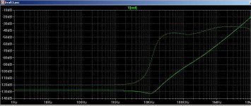
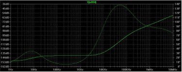
The best way to improve the performance is to parallel up more shunt capacitors on the output. Below is the simulated ripple rejection plot for an additional 470uF low ESR electrolytic - now better than 160dB at rectified line frequency (100Hz). HF output impedance is also reduced proportionally.
Cheers,
Glen
Attachments
G.Kleinschmidt said:Below is the simulated ripple rejection plot for an additional 470uF low ESR electrolytic - now better than 160dB at rectified line frequency (100Hz). HF output impedance is also reduced proportionally.
The MJE340 driver was also substituted for a KSC3505 and the 750 ohm resistive load was substituted for a 100mA current sink.
EDIT: scrap that, I'm getting mt LTspice files mixed up. That last plot shows the ripple rejection of the regulator unloaded with two parallel 470uF shunt capacitors.
G.Kleinschmidt said:Stability is rendered unconditional by the 470uF output shunt capacitor and PSRR (or ripple rejection).......
So the cap across the measuring bridge upper leg (R8) is what converts the shunt to an oscillator.G.Kleinschmidt said:Unfortunately bypassing R8 with as little as 1nF turns the circuit into an oscillator. Bypassing voltage reference V1 in a real life version would reduce reference noise, but such a bypass capacitor would be best connected between ground and the other end of R6, taking advantage of the low pass filtering effect.
Others have called this active ripple suppression.
Are you saying that adding the R8 bypass is what makes it necessary to correctly choose the output cap to avoid oscillation?
If a cap across LTP base Vref to ground is better than across V1 then why don't you add both?
Is there any way to avoid the 2 to 3mV overshoot on switching on/off the load?
This is a ClassA amp supply. It's current output will be quiescent +- the ClassA output current. In this situation the simulation should not be switching the load on/off but varying it from a fixed 100mA to sweeping/stepping from 20mA to 180mA (100+-80) since the CCS has a 180mA maximum pass current. Could stepping the output like this remove some of the apparent overshoot. 3k6 (21mA) fixed load and 510r (168mA) as switched load achieves this (470r//3k6 overloads the CCS).
G.Kleinschmidt said:
Q8 is the CCS, Q7 being its power dissipating cascode. This was done to improve the CCS’s ripple rejection. You cannot make a decent CCS with a high power transistor (high junction capacitances). Zener D2 is used as a secondary reference, buffered by Q9 to further improve the regulation of the CCS biasing voltage.
Unfortunately bypassing R8 with as little as 1nF turns the circuit into an oscillator. Bypassing voltage reference V1 in a real life version would reduce reference noise, but such a bypass capacitor would be best connected between ground and the other end of R6, taking advantage of the low pass filtering effect.
The best way to improve the performance is to parallel up more shunt capacitors on the output. Below is the simulated ripple rejection plot for an additional 470uF low ESR electrolytic - now better than 160dB at rectified line frequency (100Hz). HF output impedance is also reduced proportionally.
Cheers,
Glen
Hi Glen,
Bypassing R8 would improve output ripple rejection, and you will typically find that increasing the output capacitance will let you get away with it without instability. But it also depends on layout, ie that you take off the feedback at the load and return the ref and ref filter to a ground reference that doesn't carry load current. But why am I telling you that ? 😉
Jan Didden
AndrewT said:
So the cap across the measuring bridge upper leg (R8) is what converts the shunt to an oscillator.
Others have called this active ripple suppression.
Are you saying that adding the R8 bypass is what makes it necessary to correctly choose the output cap to avoid oscillation?
Bypassing R8 decreased the HF closed loop gain to unity. The regulator was not unity gain stable with a single 470uF output capacitor.
If a cap across LTP base Vref to ground is better than across V1 then why don't you add both?
Because it is pointless in this basic simulation.
Is there any way to avoid the 2 to 3mV overshoot on switching on/off the load?
2-3mV overshoot on a 75V is bugger all for an abrupt load on/off condition. It could be improved, but a probably won't bother.
This is a ClassA amp supply. It's current output will be quiescent +- the ClassA output current. In this situation the simulation should not be switching the load on/off but varying it from a fixed 100mA to sweeping/stepping from 20mA to 180mA (100+-80) since the CCS has a 180mA maximum pass current. Could stepping the output like this remove some of the apparent overshoot. 3k6 (21mA) fixed load and 510r (168mA) as switched load achieves this (470r//3k6 overloads the CCS).
The overshoot is due the fact that the load was switched on and off very abruptly and I tested it this way in simulation because it is an excellent way to examine the performance of the regulator. The response of the regulator is not infinitely fast so there will always be a degree of over shoot in such circumstances. But +/- several mV on +75V isn't worth worrying about.
Also, I said that this supply was designed to supply the low power circuits of my class A amp (ie the input stage / VAS / predriver / biasing circuits). These essentially draw a constant current of 80mA with no abrupt switching, so the regulator is over designed for the intended purpose.
The output stage of my class A has a Q current of 6.3A.
Cheers,
Glen
janneman said:
Hi Glen,
Bypassing R8 would improve output ripple rejection, and you will typically find that increasing the output capacitance will let you get away with it without instability. But it also depends on layout, ie that you take off the feedback at the load and return the ref and ref filter to a ground reference that doesn't carry load current. But why am I telling you that ? 😉
Jan Didden
Hi Jan
I can get the 23dB (27k/1.93k) improvement in LF ripple rejection by bypassing R8 with a suitably large capacitor, but then the output capacitance ESR becomes critical, both for stability and transient response.
I can reduce the open loop gain to make amends for this of course (larger LTP emitter resistors or emitter degeneration of the shunt transistor), and hence the negative feedback factor, but that obviously defeats the whole purpose of bypassing R8 and just gets me back to where I started! 🙁
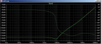
The circuit has a huge stability margin without R8 bypassed and is pretty insensitive to the output capacitance ESR and still simulates better than 140dB ripple rejection out to 15kHz with 70dB ripple rejection at 1MHz.
This is about as good (and more than good enough for the intended application 😉) as I think I can make it without making the regulator section excessively sensitive to layout and capacitor ESR.
Improving the CCS would be my preferred next step for improving the ripple rejection.
Cheers,
Glen
Hi GK,
thanks for taking the time to explain away those misconceptions of mine.
But one more.
The ClassA front end does have a variable current in the supply rails for most topologies. I cannot recall your schematic, but the VAS is the first culprit that draws a non fixed current that varies in direct proportion to the input signal, while working in single ended ClassA mode.
The pre-drivers and drivers also draw variable current from the supply rails. You are probably feeding the drivers from the main unregulated supply, but even the pre-drivers drop into ClassAB on large output currents.
Your simulation is extreme, and you are right to "test" it your way to pull out any misbehaviour. I will accept that mV overshoot on instantaneous current change is very good. Most reports would not divulge this info to allow comparison.
Well Done on what looks like a nice supply.
I'm away to breadboard a 60V version, unless there is a mk111 due out soon.
thanks for taking the time to explain away those misconceptions of mine.
G.Kleinschmidt said:But +/- several mV on +75V isn't worth worrying about.
Also, I said that this supply was designed to supply the low power circuits of my class A amp (ie the input stage / VAS / pre-driver / biasing circuits). These essentially draw a constant current of 80mA with no abrupt switching, so the regulator is over designed for the intended purpose.
The output stage of my class A has a Q current of 6.3A.
But one more.
The ClassA front end does have a variable current in the supply rails for most topologies. I cannot recall your schematic, but the VAS is the first culprit that draws a non fixed current that varies in direct proportion to the input signal, while working in single ended ClassA mode.
The pre-drivers and drivers also draw variable current from the supply rails. You are probably feeding the drivers from the main unregulated supply, but even the pre-drivers drop into ClassAB on large output currents.
Your simulation is extreme, and you are right to "test" it your way to pull out any misbehaviour. I will accept that mV overshoot on instantaneous current change is very good. Most reports would not divulge this info to allow comparison.
Well Done on what looks like a nice supply.
I'm away to breadboard a 60V version, unless there is a mk111 due out soon.
- Status
- Not open for further replies.
- Home
- Amplifiers
- Solid State
- Bob Cordell Interview: Power Supplies