andy_c said:The first configuration I looked at was an adaptation of t3g. This has a current gain of 7x in the Miller loop, and takes the Miller feedback from the emitter of an EF following the VAS. When I looked at the Miller loop gain, I was dismayed by what I saw. At around 10 MHz, its magnitude dropped like a stone, along with the phase. By the time the ULG freq was reached, the phase lag was huge, well in excess of 180 degrees. I gave up on trying to stabilize the thing, because it would have required a compensation cap of thousands of pF together with some careful lead compensation. I'm not sure how Edmond got this stable. His circuit may be an order of magnitude faster than mine, or the phase lag at the ULG freq may have just coincidentally been far from 180 degrees. I don't know. I didn't pursue it further.
[snip]
Hi Andy,
This is an interesting observation, the more so as I got a different picture. But why? One reason might be the larger (and slower) drivers you are using. Another reason might be different MOSFET models with regard to Cgd: the tanh/atan model vs the diode model.
However, there's a completely different thing that really worries me: the implementation of Middlebrooks method to simulate the loop gain as outlined by MicroCap (see: http://www.spectrum-soft.com/news/spring97/loopgain.shtm), in particular WRT the macro's. I don't thrust the results. When I revert to the old fashion methods of breaking the loop, but still combining the current respectively voltage component in the same way, I get more meaningful results.
So I wonder how reliable is the LTSpice gain probe? Is it based on exactly the same method as published by MicroCap?
Any idea?
Regards,
Edmond.
HI Edmond,
I was using the KSA1381/KSC3503 for predriver and 2SA1837/2SC4793 for drivers, so maybe the drivers are making the difference. For the FETs, |Vgd| is around 85V, so Cgd is small, but maybe the 10+10 devices are creating a much more capacitive load than in your circuit. It's hard to say.
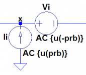
Regarding the loop gain simulations, if you have LTspice installed, the technique is described in a heavily commented file in examples\educational\loopgain2.asc. In case you don't have it, I've attached a picture of the probe below. In that picture, u() is the unit step function, and the parameter prb is specified as:
.step param prb list -1 1
So that turns the voltage and current sources on and off. The loop gain formula comes from a paper by Tian, Kundert, Visvanathan and Hantgan called "Striving for Small-Signal Stability", which is in this PDF file. Their approach extends Middlebrook's analysis to take reverse transmission (non-unilateral behavior) of the loop into account. The Tian formula for the loop gain is:
loop_gain=-1/(1-1/(2*(I(Vi)@1*V(x)@2-V(x)@1*I(Vi)@2)+V(x)@1+I(Vi)@2))
where "@1" is the first step (prb=-1) and "@2" is for prb=1. With this approach the probe can be reversed and one still gets the same answer for the loop gain. The disadvantage of this approach is that no other .STEP variables can be used when simulating loop gain. I've tried comparing loop gain results using Middlebrook's formula and the Tian formula and not found significant differences, but this was with global, not Miller loop gain.
This all came about in a discussion led by Frank Wiedmann in the Yahoo LTspice users' group. He has a very interesting web page devoted to loop gain issues and Middlebrook's "General Feedback Theorem" here.
I was using the KSA1381/KSC3503 for predriver and 2SA1837/2SC4793 for drivers, so maybe the drivers are making the difference. For the FETs, |Vgd| is around 85V, so Cgd is small, but maybe the 10+10 devices are creating a much more capacitive load than in your circuit. It's hard to say.
Regarding the loop gain simulations, if you have LTspice installed, the technique is described in a heavily commented file in examples\educational\loopgain2.asc. In case you don't have it, I've attached a picture of the probe below. In that picture, u() is the unit step function, and the parameter prb is specified as:
.step param prb list -1 1
So that turns the voltage and current sources on and off. The loop gain formula comes from a paper by Tian, Kundert, Visvanathan and Hantgan called "Striving for Small-Signal Stability", which is in this PDF file. Their approach extends Middlebrook's analysis to take reverse transmission (non-unilateral behavior) of the loop into account. The Tian formula for the loop gain is:
loop_gain=-1/(1-1/(2*(I(Vi)@1*V(x)@2-V(x)@1*I(Vi)@2)+V(x)@1+I(Vi)@2))
where "@1" is the first step (prb=-1) and "@2" is for prb=1. With this approach the probe can be reversed and one still gets the same answer for the loop gain. The disadvantage of this approach is that no other .STEP variables can be used when simulating loop gain. I've tried comparing loop gain results using Middlebrook's formula and the Tian formula and not found significant differences, but this was with global, not Miller loop gain.
This all came about in a discussion led by Frank Wiedmann in the Yahoo LTspice users' group. He has a very interesting web page devoted to loop gain issues and Middlebrook's "General Feedback Theorem" here.
Attachments
andy_c said:HI Edmond,
I was using the KSA1381/KSC3503 for predriver and 2SA1837/2SC4793 for drivers, so maybe the drivers are making the difference. For the FETs, |Vgd| is around 85V, so Cgd is small, but maybe the 10+10 devices are creating a much more capacitive load than in your circuit. It's hard to say.
Hi Andy.
Have you tried lowering the transition frequency to account for the fT droop?
Cheers,
Glen
Hi Glen,
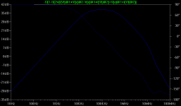
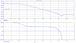
Just to clarify, I'm looking not at the global loop gain of the amp, but the Miller loop gain of this configuration (with TMC disabled). That loop gain looks as below. Reducing the ULG freq of the Miller loop is done by either increasing C6 and C7 or reducing C4 and C5 or both. But C6 and C7 are already 470p, which is pretty large, and C4 and C5 are 84p, which is normal.
As you can see, there's just too darned much loop gain at high frequencies, and lots of phase lag to boot. And this plot includes the lead compensation provided by R10 and R11 as well. It's something that I just can't work with.
Attachments
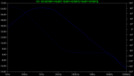
In contrast, here is the CMCL version, taken from this schematic. This looks great, about as good as one could ever expect.
Attachments
andy_c said:In contrast, here is the CMCL version, taken from this schematic. This looks great, about as good as one could ever expect.
OK, now I see.
I assue the excess loop gain in the non-CMCL version is due to the fact that the TMC is taken from the pre-driver emitters, not the VAS collectors as in the CMCL version?
What effect does shifting (in the non-CMCL version) R17 and R18 to V5 instead of R19 have?
Cheers,
Glen
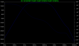
Good idea. Here is the result. Better? 🙂 I had to reduce the lead compensation resistors R10 and R11 as there was too much lead compensation. I left C6 and C7 as-is, and you can see that at 470p they are way too large and that it's overcompensated. I sure don't like the looks of what happens when Miller comp is taken from an EF following the VAS.
Attachments
Another interesting thing is that the CMCL version has over 50 dB of loop gain at 20 kHz. Once the non-CMCL version is made stable, it gets beaten hands down in the loop gain department.
Isn't that the whole point of a CMCL? 🙂 You get rid of that load resistor on the input stage.
Cheers,
Glen
Cheers,
Glen
G.Kleinschmidt said:Hey! how about the loop gain and phase margin of the CMCL loop itself?
🙂
Hi Glen,
Nothing to worry about, see below.
Notice: C10 should be ~3n3, not 33n.
Regards,
Edmond.
Attachments
Edmond Stuart said:
Hi Glen,
Nothing to worry about, see below.
Notice: C10 should be ~3n3, not 33n.
Regards,
Edmond.
Hi Edmond.
Why not delete C10 (PSRR?) and shunt R14 and R16 instead?
Cheers,
Glen
cap
Hi Glen,
Good question. C10 has another function as well. With this cap (value not critical) you get a better better (cleaner) step response. The downside is indeed poorer PSRR at HF. So you have to decouple the supply rails (at least for the VASes) sufficiently.
Regards,
Edmond.
edit: for decoupling see also the schematic of the PGP front-end (PCB version): R1, C1, C2, R71, C29, C30 and C27.
http://home.tiscali.nl/audio/FrontEndSchPcb.html
In this schematic 'C10' is denoted as C11
G.Kleinschmidt said:Hi Edmond.
Why not delete C10 (PSRR?) and shunt R14 and R16 instead?
Cheers,
Glen
Hi Glen,
Good question. C10 has another function as well. With this cap (value not critical) you get a better better (cleaner) step response. The downside is indeed poorer PSRR at HF. So you have to decouple the supply rails (at least for the VASes) sufficiently.
Regards,
Edmond.
edit: for decoupling see also the schematic of the PGP front-end (PCB version): R1, C1, C2, R71, C29, C30 and C27.
http://home.tiscali.nl/audio/FrontEndSchPcb.html
In this schematic 'C10' is denoted as C11
Re: cap
OK, thanks Edmond.
Hmmm....... what does that 3.3nF do to the clipping recovery/performance though?
The need to remove excess charge from a cap that big is going to cause some sticking issues?
In a practical implementation, as well as adequate supply rail decoupling, this CMCL thingie will need a nfb VAS clamp too - ?
Cheers,
Glen
Edmond Stuart said:
Hi Glen,
Good question. C10 has another function as well. With this cap (value not critical) you get a better better (cleaner) step response. The downside is indeed poorer PSRR at HF. So you have to decouple the supply rails (at least for the VASes) sufficiently.
Regards,
Edmond.
edit: for decoupling see also the schematic of the PGP front-end (PCB version): R1, C1, C2, R71, C29, C30 and C27.
http://home.tiscali.nl/audio/FrontEndSchPcb.html
In this schematic 'C10' is denoted as C11
OK, thanks Edmond.
Hmmm....... what does that 3.3nF do to the clipping recovery/performance though?
The need to remove excess charge from a cap that big is going to cause some sticking issues?
In a practical implementation, as well as adequate supply rail decoupling, this CMCL thingie will need a nfb VAS clamp too - ?
Cheers,
Glen
Re: Re: cap
Hi Glen,
That 3n3 cap doesn't impair the recovery/performance and in a well designed amp an adequate supply rail decoupling will be necessary anyhow.
Also a nfb VAS clamp has little to with that CMCL 'thingie'.
In the PGP amp a nfb VAS clamp was needed to prevent overcharging of the NDFL caps during clipping, while in the PMP amp a traditional clamp is useless because the OPS has some gain (1.3x) and the front-end has its own (read: independent) power supply. As stated on my website:
"One may wonder why doing it the hard way? The answer is that this approach precisely detects where (the driver) and why (saturation) it goes wrong at the onset of clipping. One more reason is that it works completely independent of the VAS supply voltage or component tolerances. Opposed to a more conventional approach, the VAS hasn't to 'guess' when the output stage runs out of steam. "
Regards,
Edmond.
G.Kleinschmidt said:OK, thanks Edmond.
Hmmm....... what does that 3.3nF do to the clipping recovery/performance though?
The need to remove excess charge from a cap that big is going to cause some sticking issues?
In a practical implementation, as well as adequate supply rail decoupling, this CMCL thingie will need a nfb VAS clamp too - ?
Cheers,
Glen
Hi Glen,
That 3n3 cap doesn't impair the recovery/performance and in a well designed amp an adequate supply rail decoupling will be necessary anyhow.
Also a nfb VAS clamp has little to with that CMCL 'thingie'.
In the PGP amp a nfb VAS clamp was needed to prevent overcharging of the NDFL caps during clipping, while in the PMP amp a traditional clamp is useless because the OPS has some gain (1.3x) and the front-end has its own (read: independent) power supply. As stated on my website:
"One may wonder why doing it the hard way? The answer is that this approach precisely detects where (the driver) and why (saturation) it goes wrong at the onset of clipping. One more reason is that it works completely independent of the VAS supply voltage or component tolerances. Opposed to a more conventional approach, the VAS hasn't to 'guess' when the output stage runs out of steam. "
Regards,
Edmond.
andy_c said:The first configuration I looked at was an adaptation of t3g. This has a current gain of 7x in the Miller loop, and takes the Miller feedback from the emitter of an EF following the VAS. When I looked at the Miller loop gain, I was dismayed by what I saw. At around 10 MHz, its magnitude dropped like a stone, along with the phase. By the time the ULG freq was reached, the phase lag was huge, well in excess of 180 degrees. I gave up on trying to stabilize the thing, because it would have required a compensation cap of thousands of pF together with some careful lead compensation. I'm not sure how Edmond got this stable. His circuit may be an order of magnitude faster than mine, or the phase lag at the ULG freq may have just coincidentally been far from 180 degrees. I don't know. I didn't pursue it further.
[snip]
Hi Andy,
So the VAS was definitely unstable, that is, according to the gain/phase response obtained by using the LT gain probe.
But what about the overall performance of the OPS and the behavior of the global NFB loop? I'm asking this, because I have issues with (the implementation of) Middlebrooks method (more on this later).
Regards,
Edmond.
andy_c said:[snip]
Next, I looked at an adaptation of t3f, in which CMCL is used and Miller compensation is taken from the VAS collector. The Miller loop gain of this configuration looked great. Only a small compensation cap of 100 pF was required, and putting a small resistor in series with it resulted in the phase shift of the Miller loop gain being a constant -90 degrees out to 10 MHz. Even at 100 MHz, its phase shift only reached -140 degrees. Nice.
When I tried a THD-20k sim of this, I got about 40 ppm at 400W into 8 Ohms (80V peak) without using TMC. This is the same as what I got with the configuration I was previously using, shown in this post. The difference of course is that the high Miller loop current gain of the CMCL configuration allows TMC to do its thing with the potential of further distortion reduction. When I tried TMC, I was able to get this down to a little above 20 ppm. I am including 19 harmonics in this sim, so it's overly conservative.
However, TMC causes a problem in my circuit that probably doesn't show up in lower power designs. Because of the 10+10 output devices, the output stage bandwidth varies radically from its maximum value of about 20 MHz at 0VDC out, to about 2 MHz at 80VDC out. This is of course due to the Cgd variation of the vertical FETs. When it's put into a TMC loop, the overall global phase margin degrades quite a bit as the output approaches the rail. I test this behavior by simulating a 1 kHz input signal that drives the output to 80V peak, and superimpose on that a 20 kHz square wave that gives an additional output swing of 1 Volt above that. With the input LPF disabled, the square wave shows very bad ringing at the 80V peak of the sine. This goes away when TMC is disabled.
[snip]
Hi Andy,
I have observed the same problem when the output approaches the rail, at least with this circuit. But I have warned you that -to establish a level playing field- the various topologies were not individually tweaked for best performance and stability.
As a matter of fact, the TMC+CMCL version can be made much better, but on the other hand, it's also true that any attempt to reduce the distortion will result in less stability. There is no free lunch.

Regards,
Edmond.
loop gain
Hi Andy,
As said already, the additional load from more OP-devices isn't the only reason of the instability, as the 4+4 version wasn't stable either. Simply because it wasn't optimized for that specific configuration.
First, thanks for explanation and the refs. A few of them are new for me (and I have to digest them first).
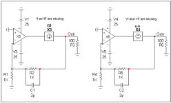
Regrettably, I can't easily implement Tian's method or Middlebrook's GFT method in MicroCap, because multiple passes on the same schematic (i.e. as needed for a gain probe) isn't supported. The only way is using three! copies. So I stick with the double injection method (thus only two copies needed, boring enough).
BTW, I don't think that omitting the calculation of the reverse-loop transmission is the real cause of my unreliable looking results.
Anyhow, my first step is getting Middlebrook's double injection method right. Therefore I would kindly ask you to have look (again) at this MicroCap's paper: http://www.spectrum-soft.com/news/spring97/loopgain.shtm and tell me how you would place the macro's in the schematic below, i.e. the position of II and IF, resp. VI and VF.
Thanks in advance.
Regards,
Edmond.
andy_c said:HI Edmond,
I was using the KSA1381/KSC3503 for predriver and 2SA1837/2SC4793 for drivers, so maybe the drivers are making the difference. For the FETs, |Vgd| is around 85V, so Cgd is small, but maybe the 10+10 devices are creating a much more capacitive load than in your circuit. It's hard to say.
Hi Andy,
As said already, the additional load from more OP-devices isn't the only reason of the instability, as the 4+4 version wasn't stable either. Simply because it wasn't optimized for that specific configuration.
Regarding the loop gain simulations, if you have LTspice installed, the technique is described in a heavily commented file in examples\educational\loopgain2.asc. In case you don't have it, I've attached a picture of the probe below. In that picture, u() is the unit step function, and the parameter prb is specified as:
.step param prb list -1 1
So that turns the voltage and current sources on and off. The loop gain formula comes from a paper by Tian, Kundert, Visvanathan and Hantgan called "Striving for Small-Signal Stability", which is in this PDF file. Their approach extends Middlebrook's analysis to take reverse transmission (non-unilateral behavior) of the loop into account. The Tian formula for the loop gain is:
loop_gain=-1/(1-1/(2*(I(Vi)@1*V(x)@2-V(x)@1*I(Vi)@2)+V(x)@1+I(Vi)@2))
where "@1" is the first step (prb=-1) and "@2" is for prb=1. With this approach the probe can be reversed and one still gets the same answer for the loop gain. The disadvantage of this approach is that no other .STEP variables can be used when simulating loop gain. I've tried comparing loop gain results using Middlebrook's formula and the Tian formula and not found significant differences, but this was with global, not Miller loop gain.
This all came about in a discussion led by Frank Wiedmann in the Yahoo LTspice users' group. He has a very interesting web page devoted to loop gain issues and Middlebrook's "General Feedback Theorem" here.
First, thanks for explanation and the refs. A few of them are new for me (and I have to digest them first).
Regrettably, I can't easily implement Tian's method or Middlebrook's GFT method in MicroCap, because multiple passes on the same schematic (i.e. as needed for a gain probe) isn't supported. The only way is using three! copies. So I stick with the double injection method (thus only two copies needed, boring enough).
BTW, I don't think that omitting the calculation of the reverse-loop transmission is the real cause of my unreliable looking results.
Anyhow, my first step is getting Middlebrook's double injection method right. Therefore I would kindly ask you to have look (again) at this MicroCap's paper: http://www.spectrum-soft.com/news/spring97/loopgain.shtm and tell me how you would place the macro's in the schematic below, i.e. the position of II and IF, resp. VI and VF.
Thanks in advance.
Regards,
Edmond.
Attachments
- Home
- Amplifiers
- Solid State
- Bob Cordell Interview: Negative Feedback