talking?
Hi Dimitri,
I'm afraid not really, as I assume that syn08 is more interested in the accessibility of his website than in my comments.
Cheers,
Edmond.
dimitri said:look, they are talking to each other
Hi Dimitri,
I'm afraid not really, as I assume that syn08 is more interested in the accessibility of his website than in my comments.
Cheers,
Edmond.
Edmond and Syn08,
It's nice to have both of you back! Happy New Year!
Here's to properly-designed negative feedback circuits!
Cheers,
Bob
It's nice to have both of you back! Happy New Year!
Here's to properly-designed negative feedback circuits!
Cheers,
Bob
Bob Cordell said:Edmond and Syn08,
It's nice to have both of you back! Happy New Year!
Here's to properly-designed negative feedback circuits!
Cheers,
Bob
Thanks Bob,
I wish you a Happy New Year as well and more positive FB on negative FB. 🙂
Cheers,
Edmond.
Bob Cordell said:Edmond and Syn08,
It's nice to have both of you back! Happy New Year!
Here's to properly-designed negative feedback circuits!
Cheers,
Bob
Happy New Year Bob!
To paraphrase Carl Zwanzig, Negative Feedback is like the Force. It has a light side, a dark side, and it holds the Universe together.
syn08 said:
Happy New Year Bob!
To paraphrase Carl Zwanzig, Negative Feedback is like the Force. It has a light side, a dark side, and it holds the Universe together.
syn08
Shouldn’t you work on your website accessibility?
Maybe it’s the dark forces, the moon phase or even the negative influence by the Mars moons? Or maybe it is just Joshua and his friends.
Spooky
Stinius

Originally posted by Edmond Stuart ........
If routed via: 'Netherland, Amsterdam, Support Net'
I got 'Not Found'. Also when using your IP address (66.6.63.32)
But if routed via 'Greece, Athens, NTUA - National Technical University of Athens' (for example) I got no error msg.
So, ''Netherland, Amsterdam, Support Net' has issues. But why?
...................
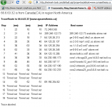
Support Net (Amsterdam) doesn't work apparently due to another bug. Using a different trace tool (network-tools.com), it seems that the connection gets stuck in Ottawa (see picture) and not in Amsterdam. This also explains why people from other countries have problems as well.
Attachments
Slightly less OT:
Yokagawa have introduced a new 2-channel curve tracer interfaced directly to a PC, the GS820:
http://www.planetanalog.com/showArticle.jhtml?articleID=212700339&cid=NL_planet
They quoted me a price of around euro 12k. Not really a diy price. Maybe a group buy 😉
Jan Didden
Yokagawa have introduced a new 2-channel curve tracer interfaced directly to a PC, the GS820:
http://www.planetanalog.com/showArticle.jhtml?articleID=212700339&cid=NL_planet
They quoted me a price of around euro 12k. Not really a diy price. Maybe a group buy 😉
Jan Didden
janneman said:Slightly less OT:
Yokagawa have introduced a new 2-channel curve tracer interfaced directly to a PC, the GS820:
http://www.planetanalog.com/showArticle.jhtml?articleID=212700339&cid=NL_planet
They quoted me a price of around euro 12k. Not really a diy price. Maybe a group buy 😉
Jan Didden
Hi Jan,
That's an interesting idea to build a curve tracer employing PC infrastructure. Maybe a good DIY project. I could almost imagine one that would be quite inexpensive employing some DACs, ADCs, a PIC processor and some controllable power supplies that might do the trick for most applications.
Cheers,
Bob
There wass a guy on the ETF 2007 who had build one (for tubes) just using a sound card and PC software. A sound card is basically a bunch of AD and DA converters and some other stuff. It looked quite neat, I'll see if I can find it. By a French guy. Maybe Stuart will remember it.
Edit: the picture is here:
http://www.triodefestival.net/index.php?page=tube-curves-tracer , and there is a link to the design at the bottom of the page. The software source code is free....
Jan Didden
Edit: the picture is here:
http://www.triodefestival.net/index.php?page=tube-curves-tracer , and there is a link to the design at the bottom of the page. The software source code is free....
Jan Didden
More on sticking and clipping performance.
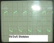
Here is a scope shot of my K12A amplifier clipping at 10kHz.
I did not bother with a voltage clamp on the VAS collector in this basic design, and allow the pre driver transistors to saturate - though a simple diode clamp on the VAS buffer base acts as a VAS current limiter (2*Iq) and prevents saturation of the VAS cascode transistors.
Saturation of the BC546/BC556 pre-driver transistor pair results in approximately 1uS of sticking.
TMC (1.1MHz ULG) is used and the amp does ~0.002% THD-20 into 4 ohms. A previous prototype version with supply rails scaled for 12W into 8 ohms did ~0.001% THD-20.
I believe this is the first scope shot of a TMC amplifier to grace the pages of DIY audio 😀 😀
Cheers,
Glen
Attachments
Re: More on sticking and clipping performance.
These are nice results, Glen. TMC is quite effective.
What slew rate do you achieve?
What input stage tail current are you running?
What output stage bias current are you running?
Cheers,
Bob
G.Kleinschmidt said:Here is a scope shot of my K12A amplifier clipping at 10kHz.
I did not bother with a voltage clamp on the VAS collector in this basic design, and allow the pre driver transistors to saturate - though a simple diode clamp on the VAS buffer base acts as a VAS current limiter (2*Iq) and prevents saturation of the VAS cascode transistors.
Saturation of the BC546/BC556 pre-driver transistor pair results in approximately 1uS of sticking.
TMC (1.1MHz ULG) is used and the amp does ~0.002% THD-20 into 4 ohms. A previous prototype version with supply rails scaled for 12W into 8 ohms did ~0.001% THD-20.
I believe this is the first scope shot of a TMC amplifier to grace the pages of DIY audio 😀 😀
Cheers,
Glen
These are nice results, Glen. TMC is quite effective.
What slew rate do you achieve?
What input stage tail current are you running?
What output stage bias current are you running?
Cheers,
Bob
Re: Re: More on sticking and clipping performance.
Hi Bob
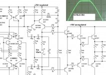
1) ~35V/us
More than enough for such a low voltage amplifier - 250kHz squarewave response attached. The output network is a 2-pole L//R-C low pass filter. The ripple in the response is due to the 1uH (in parallel with 1R) output inductor resonating with the 100nF output capacitor.
2) 5mA
3) 1.5A
The amp clips at 12V (18W), so I run the bias high enough to keep it in class A into 4 ohms 'till clipping.
Cheers,
Glen
Bob Cordell said:
These are nice results, Glen. TMC is quite effective.
What slew rate do you achieve?
What input stage tail current are you running?
What output stage bias current are you running?
Cheers,
Bob
Hi Bob
1) ~35V/us
More than enough for such a low voltage amplifier - 250kHz squarewave response attached. The output network is a 2-pole L//R-C low pass filter. The ripple in the response is due to the 1uH (in parallel with 1R) output inductor resonating with the 100nF output capacitor.
2) 5mA
3) 1.5A
The amp clips at 12V (18W), so I run the bias high enough to keep it in class A into 4 ohms 'till clipping.
Cheers,
Glen
Attachments
Nfb-ops
Recently there were some discussions on the YAP thread how to modify front-end of the NFB-OPS in such a way that it's capable of driving 10 pairs of MOSFETs (Andy_C). Since the simple version is clearly running out of steam, one have three options: Increasing the current gain of the VAS (actually a current mirror), adding an extra driver (an emitter follower) or doing both. As I was wondering about the effect on distortion I've simulated seven basics variants: with and without the following components:
- An emitter follower before the VAS (EF1).
- A cascode after the VAS.
- An additional emitter follower after the VAS (EF2)
- Increased current gain of the VAS by a factor of 7 (Andy_C's idea)
- Increased current gain of the VAS to about 800 by adding a common mode control loop
BTW, I've not tried all possible combinations, only seven of them.
Since I was more interested in the relative performance I've loaded the front-end with four pair of MOSFETs in the OPS instead of ten.
To ease the comparison of THD figures I've kept in all cases the global unity loop gain frequency at 2.5MHz.
Where the VAS current gain was boosted, it was necessary to add a lead-lag compensation at the VAS input as well.
Furthermore, the simulations were repeated with a transitional Miller compensation (TMC) instead of a simple compensation.
Legend:
EF1: 1st emitter follower
EF2: 2nd emitter follower
G-VAS: current gain of the VAS
CMCL: common mode control loop
THD-4: distortion in ppm @20kHz an 30Vpk into 4 Ohm
THD-NL: dito, but without load
PM-G: phase margin in degrees of the global FB loop
GM-G: gain margin in dB of the global FB loop
PM-M: phase margin in degrees of the Miller FB loop
GM-M: gain margin in dB of the Miller FB loop
CLC: the capacitance in nF, directly tied to the output at which the circuit starts oscillating.
Note: THD-NL has been added to identify where the distortion stems from: front-end vs OPS.
CLC has been added as rough indicator of the stability.
The results without TMC:
The THD20 figures under load conditions don't give a clear clue about the most favorable topology, apparently due to dominance of OPS distortion.
The only interesting thing is that if the cascode (see t1d) is replaced by an emitter follower at the VAS input (see t1e), we get the same THD20.
Apparently the impact of the Early effect and Cob is reduced due to the low impedance at the VAS input.
The THD20 figures with no load however, reveal a very different picture. The more gain around the Miller loop, the less distortion of the front-end.
Is this important? Yes!, as it appears to be necessary to enable further improvements by means TMC, see next table:
The results with TMC
Now it becomes obvious in which direction to go: the more VAS or driver current gain, the lower the distortion.
The clear winner is t3g (increased VAS gain + pre-driver) directly followed by t3f (CMCL version).
Although t3g has slightly lower distortion, it is less stable, probably because of the additional gain stage EF2.
Also notice the bad performance of t3a. As already elsewhere stated TMC is incompatible with a low gain VAS. In this example it doubles the distortion to 48ppm (are you listening syn08?).
Disclaimer: These are only relative figures and will probably not reflect the performance in real life. They are only meant as guidance as to which direction to go.
Regards,
Edmond.
Recently there were some discussions on the YAP thread how to modify front-end of the NFB-OPS in such a way that it's capable of driving 10 pairs of MOSFETs (Andy_C). Since the simple version is clearly running out of steam, one have three options: Increasing the current gain of the VAS (actually a current mirror), adding an extra driver (an emitter follower) or doing both. As I was wondering about the effect on distortion I've simulated seven basics variants: with and without the following components:
- An emitter follower before the VAS (EF1).
- A cascode after the VAS.
- An additional emitter follower after the VAS (EF2)
- Increased current gain of the VAS by a factor of 7 (Andy_C's idea)
- Increased current gain of the VAS to about 800 by adding a common mode control loop
BTW, I've not tried all possible combinations, only seven of them.
Since I was more interested in the relative performance I've loaded the front-end with four pair of MOSFETs in the OPS instead of ten.
To ease the comparison of THD figures I've kept in all cases the global unity loop gain frequency at 2.5MHz.
Where the VAS current gain was boosted, it was necessary to add a lead-lag compensation at the VAS input as well.
Furthermore, the simulations were repeated with a transitional Miller compensation (TMC) instead of a simple compensation.
Legend:
EF1: 1st emitter follower
EF2: 2nd emitter follower
G-VAS: current gain of the VAS
CMCL: common mode control loop
THD-4: distortion in ppm @20kHz an 30Vpk into 4 Ohm
THD-NL: dito, but without load
PM-G: phase margin in degrees of the global FB loop
GM-G: gain margin in dB of the global FB loop
PM-M: phase margin in degrees of the Miller FB loop
GM-M: gain margin in dB of the Miller FB loop
CLC: the capacitance in nF, directly tied to the output at which the circuit starts oscillating.
Note: THD-NL has been added to identify where the distortion stems from: front-end vs OPS.
CLC has been added as rough indicator of the stability.
The results without TMC:
Code:
[size=3]EF1   G-VAS   cascode   EF2   CMCL  THD-4  THD-NL   PM-G GM-G   PM-M GM-M  CLC   schematic
 N      1x       Y       N     N    23.0    31.8     80   25     na   20   150     [url=http://home.tiscali.nl/data.odyssey/t1a.html]t1a[/url]
 N      7x       Y       N     N    20.4     5.3     81   27     98   34    90     [url=http://home.tiscali.nl/data.odyssey/t1b.html]t1b[/url]
 N      1x       N       Y     N    22.3    12.9     79   21     62   16   120     [url=http://home.tiscali.nl/data.odyssey/t1c.html]t1c[/url]
 N      1x       Y       Y     N    17.5     8.9     80   22     53   9.4  150     [url=http://home.tiscali.nl/data.odyssey/t1d.html]t1d[/url]
 Y      1x       N       Y     N    17.3     7.4     79   21     61   15   140     [url=http://home.tiscali.nl/data.odyssey/t1e.html]t1e[/url]
 Y    800x       N       N     Y    20.9     1.6     74   28     94   27   120     [url=http://home.tiscali.nl/data.odyssey/t1f.html]t1f[/url]
 Y      7x       N       Y     N    21.5     1.6     80   24     57   20   140     [url=http://home.tiscali.nl/data.odyssey/t1g.html]t1g[/url] [/size]
The THD20 figures under load conditions don't give a clear clue about the most favorable topology, apparently due to dominance of OPS distortion.
The only interesting thing is that if the cascode (see t1d) is replaced by an emitter follower at the VAS input (see t1e), we get the same THD20.
Apparently the impact of the Early effect and Cob is reduced due to the low impedance at the VAS input.
The THD20 figures with no load however, reveal a very different picture. The more gain around the Miller loop, the less distortion of the front-end.
Is this important? Yes!, as it appears to be necessary to enable further improvements by means TMC, see next table:
The results with TMC
Code:
[size=3]EF1   G-VAS   cascode   EF2   CMCL  THD-4  THD-NL   PM-G GM-G    CLC   schematic
 N      1x       Y       N     N    47.8    32.4     71   27     >1u     [url=http://home.tiscali.nl/data.odyssey/t3a.html]t3a[/url]
 N      7x       Y       N     N    14.8     5.2     81   27      68     [url=http://home.tiscali.nl/data.odyssey/t3b.html]t3b[/url]
 N      1x       N       Y     N    13.2    12.9     82   21      56     [url=http://home.tiscali.nl/data.odyssey/t3c.html]t3c[/url]
 N      1x       Y       Y     N     8.8     8.9     83   22      47     [url=http://home.tiscali.nl/data.odyssey/t3d.html]t3d[/url]
 Y      1x       N       Y     N     6.3     7.2     82   21      56     [url=http://home.tiscali.nl/data.odyssey/t3e.html]t3e[/url]
 Y    800x       N       N     Y     3.3     1.5     71   27      82     [url=http://home.tiscali.nl/data.odyssey/t3f.html]t3f[/url]
 Y      7x       N       Y     N     2.6     1.5     83   23      44     [url=http://home.tiscali.nl/data.odyssey/t3g.html]t3g[/url] [/size]
Now it becomes obvious in which direction to go: the more VAS or driver current gain, the lower the distortion.
The clear winner is t3g (increased VAS gain + pre-driver) directly followed by t3f (CMCL version).
Although t3g has slightly lower distortion, it is less stable, probably because of the additional gain stage EF2.
Also notice the bad performance of t3a. As already elsewhere stated TMC is incompatible with a low gain VAS. In this example it doubles the distortion to 48ppm (are you listening syn08?).
Disclaimer: These are only relative figures and will probably not reflect the performance in real life. They are only meant as guidance as to which direction to go.
Regards,
Edmond.
Re: Nfb-ops
Hi Edmond,
This looks like a very nice investigation, although I have not yet had a chance to fully review and understand it. I have a couple of questions with regard to what is the starring point reference design on which you make these various changes.
Is the reference design what we would call an output Double, or Darlinton, where we have a driver driving the MOSFETs, and where in your EF2 change, you basically make the output stage into a Triple, where two cascaded EF's (pre-driver and driver) drive the MOSFETs?
Is the reference design one where the LTP basically drives directly the VAS transistor, and where your addition of EF1 makes the VAS into what some of us would call a Darlington VAS?
My own experience mirrors some of yours. The use of a Darlington VAS (actually, just an EF in front of the VAS transistor), does reduce the Early effect of the VAS, and tends to give more bang for the buck than a cascode instead. In other words, beef up the VAS current gain with the EF1 before you make the VAS into a cascode. Secondly, just as with BJT output stages, going to a Triple output stage structure is almost always a very good idea.
Thanks,
Bob
Edmond Stuart said:Recently there were some discussions on the YAP thread how to modify front-end of the NFB-OPS in such a way that it's capable of driving 10 pairs of MOSFETs (Andy_C). Since the simple version is clearly running out of steam, one have three options: Increasing the current gain of the VAS (actually a current mirror), adding an extra driver (an emitter follower) or doing both. As I was wondering about the effect on distortion I've simulated seven basics variants: with and without the following components:
- An emitter follower before the VAS (EF1).
- A cascode after the VAS.
- An additional emitter follower after the VAS (EF2)
- Increased current gain of the VAS by a factor of 7 (Andy_C's idea)
- Increased current gain of the VAS to about 800 by adding a common mode control loop
BTW, I've not tried all possible combinations, only seven of them.
Since I was more interested in the relative performance I've loaded the front-end with four pair of MOSFETs in the OPS instead of ten.
To ease the comparison of THD figures I've kept in all cases the global unity loop gain frequency at 2.5MHz.
Where the VAS current gain was boosted, it was necessary to add a lead-lag compensation at the VAS input as well.
Furthermore, the simulations were repeated with a transitional Miller compensation (TMC) instead of a simple compensation.
Legend:
EF1: 1st emitter follower
EF2: 2nd emitter follower
G-VAS: current gain of the VAS
CMCL: common mode control loop
THD-4: distortion in ppm @20kHz an 30Vpk into 4 Ohm
THD-NL: dito, but without load
PM-G: phase margin in degrees of the global FB loop
GM-G: gain margin in dB of the global FB loop
PM-M: phase margin in degrees of the Miller FB loop
GM-M: gain margin in dB of the Miller FB loop
CLC: the capacitance in nF, directly tied to the output at which the circuit starts oscillating.
Note: THD-NL has been added to identify where the distortion stems from: front-end vs OPS.
CLC has been added as rough indicator of the stability.
The results without TMC:
Code:[size=3]EF1 G-VAS cascode EF2 CMCL THD-4 THD-NL PM-G GM-G PM-M GM-M CLC schematic N 1x Y N N 23.0 31.8 80 25 na 20 150 [url=http://home.tiscali.nl/data.odyssey/t1a.html]t1a[/url] N 7x Y N N 20.4 5.3 81 27 98 34 90 [url=http://home.tiscali.nl/data.odyssey/t1b.html]t1b[/url] N 1x N Y N 22.3 12.9 79 21 62 16 120 [url=http://home.tiscali.nl/data.odyssey/t1c.html]t1c[/url] N 1x Y Y N 17.5 8.9 80 22 53 9.4 150 [url=http://home.tiscali.nl/data.odyssey/t1d.html]t1d[/url] Y 1x N Y N 17.3 7.4 79 21 61 15 140 [url=http://home.tiscali.nl/data.odyssey/t1e.html]t1e[/url] Y 800x N N Y 20.9 1.6 74 28 94 27 120 [url=http://home.tiscali.nl/data.odyssey/t1f.html]t1f[/url] Y 7x N Y N 21.5 1.6 80 24 57 20 140 [url=http://home.tiscali.nl/data.odyssey/t1g.html]t1g[/url] [/size]
The THD20 figures under load conditions don't give a clear clue about the most favorable topology, apparently due to dominance of OPS distortion.
The only interesting thing is that if the cascode (see t1d) is replaced by an emitter follower at the VAS input (see t1e), we get the same THD20.
Apparently the impact of the Early effect and Cob is reduced due to the low impedance at the VAS input.
The THD20 figures with no load however, reveal a very different picture. The more gain around the Miller loop, the less distortion of the front-end.
Is this important? Yes!, as it appears to be necessary to enable further improvements by means TMC, see next table:
The results with TMC
Code:[size=3]EF1 G-VAS cascode EF2 CMCL THD-4 THD-NL PM-G GM-G CLC schematic N 1x Y N N 47.8 32.4 71 27 >1u [url=http://home.tiscali.nl/data.odyssey/t3a.html]t3a[/url] N 7x Y N N 14.8 5.2 81 27 68 [url=http://home.tiscali.nl/data.odyssey/t3b.html]t3b[/url] N 1x N Y N 13.2 12.9 82 21 56 [url=http://home.tiscali.nl/data.odyssey/t3c.html]t3c[/url] N 1x Y Y N 8.8 8.9 83 22 47 [url=http://home.tiscali.nl/data.odyssey/t3d.html]t3d[/url] Y 1x N Y N 6.3 7.2 82 21 56 [url=http://home.tiscali.nl/data.odyssey/t3e.html]t3e[/url] Y 800x N N Y 3.3 1.5 71 27 82 [url=http://home.tiscali.nl/data.odyssey/t3f.html]t3f[/url] Y 7x N Y N 2.6 1.5 83 23 44 [url=http://home.tiscali.nl/data.odyssey/t3g.html]t3g[/url] [/size]
Now it becomes obvious in which direction to go: the more VAS or driver current gain, the lower the distortion.
The clear winner is t3g (increased VAS gain + pre-driver) directly followed by t3f (CMCL version).
Although t3g has slightly lower distortion, it is less stable, probably because of the additional gain stage EF2.
Also notice the bad performance of t3a. As already elsewhere stated TMC is incompatible with a low gain VAS. In this example it doubles the distortion to 48ppm (are you listening syn08?).
Disclaimer: These are only relative figures and will probably not reflect the performance in real life. They are only meant as guidance as to which direction to go.
Regards,
Edmond.
Hi Edmond,
This looks like a very nice investigation, although I have not yet had a chance to fully review and understand it. I have a couple of questions with regard to what is the starring point reference design on which you make these various changes.
Is the reference design what we would call an output Double, or Darlinton, where we have a driver driving the MOSFETs, and where in your EF2 change, you basically make the output stage into a Triple, where two cascaded EF's (pre-driver and driver) drive the MOSFETs?
Is the reference design one where the LTP basically drives directly the VAS transistor, and where your addition of EF1 makes the VAS into what some of us would call a Darlington VAS?
My own experience mirrors some of yours. The use of a Darlington VAS (actually, just an EF in front of the VAS transistor), does reduce the Early effect of the VAS, and tends to give more bang for the buck than a cascode instead. In other words, beef up the VAS current gain with the EF1 before you make the VAS into a cascode. Secondly, just as with BJT output stages, going to a Triple output stage structure is almost always a very good idea.
Thanks,
Bob
Re: Nfb-ops
Whoa! Thanks very much for that, Edmond. I was just about to start a layout of the front end board (everything up to and including the drivers), but it looks like I should try some of these configurations first. One thing that worried me about some of the ultra-low distortion topologies I've seen is that they can get pretty complex, and taming them under conditions like high slew rate can be pretty challenging. But looking at t3g, it is no more complex that my current baseline - maybe even a little simpler. Definitely worth spending some time on.
Thanks again!
Edmond Stuart said:Recently there were some discussions on the YAP thread how to modify front-end of the NFB-OPS in such a way that it's capable of driving 10 pairs of MOSFETs (Andy_C). Since the simple version is clearly running out of steam, one have three options: Increasing the current gain of the VAS (actually a current mirror), adding an extra driver (an emitter follower) or doing both. As I was wondering about the effect on distortion I've simulated seven basics variants...
Whoa! Thanks very much for that, Edmond. I was just about to start a layout of the front end board (everything up to and including the drivers), but it looks like I should try some of these configurations first. One thing that worried me about some of the ultra-low distortion topologies I've seen is that they can get pretty complex, and taming them under conditions like high slew rate can be pretty challenging. But looking at t3g, it is no more complex that my current baseline - maybe even a little simpler. Definitely worth spending some time on.
Thanks again!
Bob Cordell said:Hi Edmond,
This looks like a very nice investigation, although I have not yet had a chance to fully review and understand it. I have a couple of questions with regard to what is the starring point reference design on which you make these various changes.
Hi Bob,
The starting point reference is t1a, the most basic topologies of all.
Just click on t1a in the table below 'schematic'. My apologies; this wasn't immediately obvious.
Is the reference design what we would call an output Double, or Darlinton, where we have a driver driving the MOSFETs, and where in your EF2 change, you basically make the output stage into a Triple, where two cascaded EF's (pre-driver and driver) drive the MOSFETs?
Yes, you can see it as a triplet. BUT... the Miller take-off point has been moved from collector of the VAS to the emitter of the pre-driver. So -in this case- I prefer to call it a 'beta enhancement stage' of the VAS, analogue to EF1, as the main purpose is to increase Miller loop gain. Different views again...😉
Is the reference design one where the LTP basically drives directly the VAS transistor, and where your addition of EF1 makes the VAS into what some of us would call a Darlington VAS?
Yes indeed, except for one important difference: opposed to a real Darlington, the collectors are NOT tied together, rather the collector of the first stage is connected to a 'neutral' point.
My own experience mirrors some of yours. The use of a Darlington VAS (actually, just an EF in front of the VAS transistor), does reduce the Early effect of the VAS, and tends to give more bang for the buck than a cascode instead.
Exactly, more bang for the buck.
In other words, beef up the VAS current gain with the EF1 before you make the VAS into a cascode.
Yes, But with an 'EF1' already there, little is gained by also adding a cascode.
BTW, I learned this from D. Self. Besides, some voltage swing is lost by using a cascode.
Secondly, just as with BJT output stages, going to a Triple output stage structure is almost always a very good idea.
Thanks,
Bob
Generally speaking, you are quite right. Nevertheless, I prefer to do it in a slightly different way by concentrating extra gain inside the VAS, instead of the next stage. In a symmetrical design a bit cumbersome, but it can be solved by using a CMCL, see figure t1f or t3f. Opposed to the data from my previous post I got slightly better results with a CMCL in a more elaborate design. The devil is in the detail, so to speak.
Cheers,
Edmond.
Re: Re: Nfb-ops
Hi Andy,
You're welcome. But please be warned. The scope of my investigation is rather limited, as I was only looking at THD figures and a tiny bit to stability issues. There are much more aspects who deserve also a lot attention, like step response, clipping behavior, overload protection, bias generator etc.
Also, none of the shown topologies were tweaked. For example, t3f can be made better.
Nevertheless, I hope that my survey of various topologies will contribute to the development of your (ultimate?) amp.
Cheers,
Edmond.
andy_c said:Whoa! Thanks very much for that, Edmond. I was just about to start a layout of the front end board (everything up to and including the drivers), but it looks like I should try some of these configurations first. One thing that worried me about some of the ultra-low distortion topologies I've seen is that they can get pretty complex, and taming them under conditions like high slew rate can be pretty challenging. But looking at t3g, it is no more complex that my current baseline - maybe even a little simpler. Definitely worth spending some time on.
Thanks again!
Hi Andy,
You're welcome. But please be warned. The scope of my investigation is rather limited, as I was only looking at THD figures and a tiny bit to stability issues. There are much more aspects who deserve also a lot attention, like step response, clipping behavior, overload protection, bias generator etc.
Also, none of the shown topologies were tweaked. For example, t3f can be made better.
Nevertheless, I hope that my survey of various topologies will contribute to the development of your (ultimate?) amp.
Cheers,
Edmond.
Edmond Stuart said:
Hi Bob,
The starting point reference is t1a, the most basic topologies of all.
Just click on t1a in the table below 'schematic'. My apologies; this wasn't immediately obvious.
Yes, you can see it as a triplet. BUT... the Miller take-off point has been moved from collector of the VAS to the emitter of the pre-driver. So -in this case- I prefer to call it a 'beta enhancement stage' of the VAS, analogue to EF1, as the main purpose is to increase Miller loop gain. Different views again...😉
Yes indeed, except for one important difference: opposed to a real Darlington, the collectors are NOT tied together, rather the collector of the first stage is connected to a 'neutral' point.
Exactly, more bang for the buck.
Yes, But with an 'EF1' already there, little is gained by also adding a cascode.
BTW, I learned this from D. Self. Besides, some voltage swing is lost by using a cascode.
Generally speaking, you are quite right. Nevertheless, I prefer to do it in a slightly different way by concentrating extra gain inside the VAS, instead of the next stage. In a symmetrical design a bit cumbersome, but it can be solved by using a CMCL, see figure t1f or t3f. Opposed to the data from my previous post I got slightly better results with a CMCL in a more elaborate design. The devil is in the detail, so to speak.
Cheers,
Edmond.
Hi Edmond,
Thanks, I should have seen the place to click on the schematics. I was a bit hurried.
Yes, I often prefer to take the compensation off of the pre-driver emitter follower, especially when using TMC or TPC.
Its just lazy language that I and some others sometimes lapse into when we call the use of an emitter follower in front of a stage a Darlington; to make a VAS a true Darlington would be foolish, as the isolation from collector-base nonlinearity would be lost.
Cheers,
Bob
I've had a chance to adapt two of Edmond's above configurations to my application and look at them in detail. But first, for anybody else wondering how this all came up, I'll summarize the background briefly below.
I'd been experimenting in simulation with a high-power amp having +/- 90V rails for the output devices, and boosted, regulated rails for the rest, including drivers. I had originally been trying HEC. But over in the YAP thread, Edmond mentioned that CFB output stages with Miller comp share one very desirable trait with HEC - namely that the bandwidth of the overall output stage is not constrained by its unity loop gain frequency, but is approximately the same as that of the driver/output stage combo by itself without any feedback or HEC. In other words, for both types of circuit, the distortion gets reduced without a corresponding bandwidth reduction - a very desirable trait. After verifying this for the CFB case, I decided to try a CFB output stage. This was before Edmond posted the above circuits.
Originally, simulations consisted of THD-20k with an 80 V peak sine wave output into 8 Ohms, and a transient sim using a 160V p-p square wave that's low-pass filtered to 204 kHz to test slewing. The latter signal gives a maximum dv/dt of slightly greater than 200V/us. At first, I found that when the VAS switched into class AB mode under high-slew rate conditions, it would break into oscillation. I tracked this down to an unstable Miller loop. At first, I tried unsuccessfully to simulate the Miller loop gain. This is easy for single-ended circuits like the Blameless topology, but for a complementary circuit, having two Miller loops really messes things up. If you put the loop gain probe inside one of the two Miller loops, the simulated Miller loop gain is complete garbage. The solution to this problem involves artificially joining the two halves of the Miller loop (if possible without otherwise disturbing the circuit), and inserting the loop gain probe at the join. This technique is described in this post and shown in the schematic attached to it. Note the large inductor and capacitor in the global feedback loop to block the AC component of the global feedback. The only part of that circuit that isn't shown is the 10+10 output devices. Once I got the Miller loop compensation going, redoing the square wave simulations showed very robust performance under high-slew conditions, with the system remaining stable when the VAS switched into class AB mode. The conclusion I reached was that Miller loop stability is extremely important and should not be overlooked.
With that in mind, I looked at Edmond's t3g and t3f configurations, adapted to my power supply voltages and bias currents, with special emphasis on Miller loop stability. With regard to the effect of TMC, previous simulations I've done with a Blameless configuration and TMC show that TMC does not affect the gain or phase margin of the Miller loop when the TMC resistor is properly chosen. However, it does affect the Miller loop gain and phase at low frequencies. This is as expected. Because of this, I looked at Miller loop gain without TMC first, as it can be retrofitted later without affecting the phase and gain margins of the Miller loop.
This is getting long, so I'm going to split it into multiple posts.
The first configuration I looked at was an adaptation of t3g. This has a current gain of 7x in the Miller loop, and takes the Miller feedback from the emitter of an EF following the VAS. When I looked at the Miller loop gain, I was dismayed by what I saw. At around 10 MHz, its magnitude dropped like a stone, along with the phase. By the time the ULG freq was reached, the phase lag was huge, well in excess of 180 degrees. I gave up on trying to stabilize the thing, because it would have required a compensation cap of thousands of pF together with some careful lead compensation. I'm not sure how Edmond got this stable. His circuit may be an order of magnitude faster than mine, or the phase lag at the ULG freq may have just coincidentally been far from 180 degrees. I don't know. I didn't pursue it further.
Next, I looked at an adaptation of t3f, in which CMCL is used and Miller compensation is taken from the VAS collector. The Miller loop gain of this configuration looked great. Only a small compensation cap of 100 pF was required, and putting a small resistor in series with it resulted in the phase shift of the Miller loop gain being a constant -90 degrees out to 10 MHz. Even at 100 MHz, its phase shift only reached -140 degrees. Nice.
When I tried a THD-20k sim of this, I got about 40 ppm at 400W into 8 Ohms (80V peak) without using TMC. This is the same as what I got with the configuration I was previously using, shown in this post. The difference of course is that the high Miller loop current gain of the CMCL configuration allows TMC to do its thing with the potential of further distortion reduction. When I tried TMC, I was able to get this down to a little above 20 ppm. I am including 19 harmonics in this sim, so it's overly conservative.
However, TMC causes a problem in my circuit that probably doesn't show up in lower power designs. Because of the 10+10 output devices, the output stage bandwidth varies radically from its maximum value of about 20 MHz at 0VDC out, to about 2 MHz at 80VDC out. This is of course due to the Cgd variation of the vertical FETs. When it's put into a TMC loop, the overall global phase margin degrades quite a bit as the output approaches the rail. I test this behavior by simulating a 1 kHz input signal that drives the output to 80V peak, and superimpose on that a 20 kHz square wave that gives an additional output swing of 1 Volt above that. With the input LPF disabled, the square wave shows very bad ringing at the 80V peak of the sine. This goes away when TMC is disabled.
In the overall amplifier, which is a modified Blameless configuration, I use TMC and see the same problem with degraded phase margin near the rails. I take care of this by putting some lead compensation in the global feedback loop. This gives the global feedback loop a phase margin of about 70 degrees at 80VDC out, and is overcompensated a bit at 0VDC out, giving about a 100 degree phase margin. This gets rid of the ringing on the same test signal described above, and also eliminates ringing that was seen on recovery from clipping. I suppose I could do a similar lead compensation in the output stage's global feedback loop, but I'm worried that this could lead to very complex behavior in the overall amp, both as the output approaches clipping, and in how it recovers form clipping.
So I decided to use TMC in the VAS of the front end, but not in the output stage itself. In other words, I don't use "TMC inside of TMC". Since there will be no TMC in the output stage, the additional complexity of CMCL has no benefit, and I decided to simply go back to the output stage configuration I was using before, described here. I suspect that a CMCL-based output stage combined with TMC in the output stage would make an excellent choice for an amp that isn't burdened with so many output devices as mine is.
I have some other observations, but I'm getting tired from typing all this at the moment 🙂.
- Home
- Amplifiers
- Solid State
- Bob Cordell Interview: Negative Feedback