mikeks said:With your arrangement The major loop will be double pole while that part of the minor loop enclosing the output stage will have a triple pole roll-off. 😱
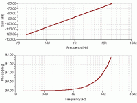
The plot of this is in my post above. In the low-frequency range, it looks like single-pole rolloff. Look at the phase also - it's an almost constant -90 deg.
Cherry
Please Mike, don't be so arrogant, Cherry is NOT a stupid guy.
Nevertheless, where can I find that paper of Dr Gift?
Cheers.
mikeks said:
I saw that examined it and found it to be nonsense, as did Dr Gift and a few others.
Please Mike, don't be so arrogant, Cherry is NOT a stupid guy.
Nevertheless, where can I find that paper of Dr Gift?
Cheers.
Re: Cherry
I've got a copy. Attachments can't be sent by using the forum's email button though - so I can't send it directly. But if you send me an email, I'll send the article to you in my reply.
estuart said:Nevertheless, where can I find that paper of Dr Gift?
I've got a copy. Attachments can't be sent by using the forum's email button though - so I can't send it directly. But if you send me an email, I'll send the article to you in my reply.
Re: Cherry
Please don't be silly.
🙄
estuart said:
Please Mike, don't be so arrogant, Cherry is NOT a stupid guy.
Nevertheless, where can I find that paper of Dr Gift?
Cheers.
Please don't be silly.
🙄
andy_c said:
The plot of this is in my post above. In the low-frequency range, it looks like single-pole rolloff. Look at the phase also - it's an almost constant -90 deg.
Hi Andy,
Why not sim. an amp with real transistors?
This will allow you to establish whether your 1st order model has any value.
Check your mail.
mikeks said:Why not sim. an amp with real transistors?
This will allow you to establish whether your 1st order model has any value.
Check your mail.
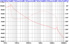
FYI, in the simplified model that I originally posted, the block labeled "out_stage" was a device-level subcircuit of the actual output stage. But the VAS and input stage were modeled as controlled sources to attempt to show the effect of the compensation mod on only output stage distortion.
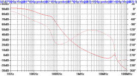
Anyway, here is the same thing, but with all device-level models for the VAS and output stage (but input stage is idealized controlled sources). This loop gain plot has the loop gain probe right after the output stage as before. It's pretty much the same, with behavior much like a single pole circuit. I don't have a satisfactory explanation for this. I've been using these idealized models for a while to try to sort out the relative distortion of the various stages, so it's been an ongoing project to make sure they agree with the device-level stuff. The full-up model has convergence problems and is a PITA to deal with.
I won't repeat the overall loop gain plot, as it looks just like my previous one, namely, the typical two-pole comp behavior.
Thanks for the email with the models.
Attachments
Re: Re: Cherry
Mike, for a while, be a nice guy. Not all Cherry's proposals are BS. NDFL for example, is a splendid idea. However, the actual implementation he has published in the past, is pretty lousy. Maybe I'll post here a simple modification that does work.
Paper of dr. Gift, where?
Cheers,
mikeks said:
Please don't be silly.
Mike, for a while, be a nice guy. Not all Cherry's proposals are BS. NDFL for example, is a splendid idea. However, the actual implementation he has published in the past, is pretty lousy. Maybe I'll post here a simple modification that does work.
Paper of dr. Gift, where?
Cheers,
Hi PMA,
That is your own circuit from 2004.
I did check it out at that time but said nothing.
This was my simulated reverse characteristic check of it.
Some posts back (above) I estimated -66dB from your own 10kHz trace.
This matches !!!
Even back then I could not be happy with quadrature damping so it just stayed on my hard-drive.
Cheers .......... Graham.
Attachments
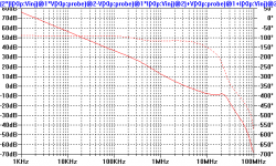
And here is the loop gain with the loop gain probe right at the amp output. Very weird! It doesn't look at all like any of the ones I posted previously. I'm not sure what this loop gain means though. That peak at 30 MHz makes it unstable.
I see what you're saying about the strangeness of this one Mike.
I see what you're saying about the strangeness of this one Mike.
Attachments
mikeks said:
You appear to forget that a DPC necessarily generates an LHP zero to cancel one of the poles....
Mike,
I didn't forget that at all. When the DPC OLG stops rolling off at 12 dB/octave, that is where the pole is that you are referring to. It is taken into account in the approximation of the overal rolloff slope of the DPC to an idealized straight line.
One thing that I need to point out is in regard to my level of conservatism in applying DPC. I am not comfortable with the phase margin dipping below about 35-40 degrees anywhere in the rolloff slope. In other words, I'm saying that if the gain were to decrease anywhere by an arbitrary amount, there would still be at least 30-40 degrees of phase margin at the resulting gain crossover point. This is why I prefer to view this form of compensation as an approximation to a constant rolloff slope of greater than 6 dB/octave.
Bob
andy_c said:
ROFL! Here's how I go about designing the thing.
Suppose you have an amp that you've determined, via single-pole comp, can have a unity loop gain frequency of 2 MHz. Of course, for single-pole comp, you'll have a loop gain of 40 dB at 20 kHz. The two-pole comp network has zero on the negative real axis. Let's put that zero at 1/10 the unity loop gain frequency. That means it will degrade the phase margin by 6 degrees (phase lag = -96 degrees at 10x the freq of the zero). A little lead comp can take care of that. In fact, Edmond's trick applied to the two-pole comp allows for just that. So now we have the open-loop zero at 200 kHz. The idealized Bode plot will have 20 dB loop gain here. Below this freq, we'll have 40 dB/dec slope. So at 20 kHz, we'll have 20 dB + 1 dec *40 dB/dec or 60 dB at 20 kHz (like my plots above). Of course, above 200 kHz the two-pole comp is no better than the single-pole. But for 19+20 kHz IM, I would think the two-pole comp would have a 20 dB advantage.
Hi Andy,
Yes, I was being conservative. As I said above, I prefer not to see phase margin be less than 30-40 degrees anywhere. I was also being conservative with respect to your calculation in assuming a 1 MHz gain crossover as opposed to your 2 MHz gain crossover. That one extra octave at 12 dB/octave makes a big difference.
You are exactly right about 19+20 kHz IM - and I should have caught that because twin-tone IM is one of my favorite tests.
Bob
Bob Cordell said:Hi Andy,
Yes, I was being conservative. As I said above, I prefer not to see phase margin be less than 30-40 degrees anywhere. I was also being conservative with respect to your calculation in assuming a 1 MHz gain crossover as opposed to your 2 MHz gain crossover. That one extra octave at 12 dB/octave makes a big difference.
You are exactly right about 19+20 kHz IM - and I should have caught that because twin-tone IM is one of my favorite tests.
Well, I picked 2 MHz because I thought that's what your amp does 🙂.
Regarding gain variations, I think the big hit is with input stage gm. I don't think I'd use undegenerated FETs here. Just using a 2N5457 as an example, its gm varies by a factor of 5 in the data sheet (1000-5000 umhos). I don't think I'd want that even with single-pole comp: five-to-one GBW variation - yuck! With regard to VAS output impedance, this variation causes weird things to happen at low frequencies (peaking in open-loop gain, etc), but this effect goes away at high frequencies. So I think if gm is well controlled, things should be okay.
andy_c said:
Well, I picked 2 MHz because I thought that's what your amp does 🙂.
Regarding gain variations, I think the big hit is with input stage gm. I don't think I'd use undegenerated FETs here. Just using a 2N5457 as an example, its gm varies by a factor of 5 in the data sheet (1000-5000 umhos). I don't think I'd want that even with single-pole comp: five-to-one GBW variation - yuck! With regard to VAS output impedance, this variation causes weird things to happen at low frequencies (peaking in open-loop gain, etc), but this effect goes away at high frequencies. So I think if gm is well controlled, things should be okay.
Problem is, once you have degenerated your input stage jfet to such a degree the net gm will be lousy and you'll need a really high impedance load to get a decent degree of voltage gain out of the stage.
A bjt differential pair, with an appropiate tail current, degenerated to the same gm as an un-degenerated jfet will will not only have a much more controlled gm, but vastly superior linearity as well.
If you want really now noise from BJT’s, it’s hard to beat the MAT03/04 pairs (or the cheaper SSM devices). Just make sure that you cascode them though, as these low noise BJT’s have high c-b capacitance. These are what I've decided to use in my current design.
Jfets are icky!

G.Kleinschmidt said:Problem is, once you have degenerated your input stage jfet to such a degree the net gm will be lousy
Yup . I should have said "I don't think I'd use FETs here" 🙂.
andy_c said:And here is the loop gain with the loop gain probe right at the amp output. Very weird! It doesn't look at all like any of the ones I posted previously. I'm not sure what this loop gain means though. That peak at 30 MHz makes it unstable.
I see what you're saying about the strangeness of this one Mike.
Hi Andy,
It becomes reasonably straightforward to appreciate when you consider that you cannot determine the total loop transmission applied about the output stage, when the later is included in the minor loop, by merely plotting the amp's major loop gain.
This is because the feedback around the output stage now has a component applied by the minor loop which is necessarily not expressed in the major loop's transmission.
Therefore, in order to determine the stability or lack thereof of that loop in which the output stage is enclosed, while taking into account the effect of the major loop, the loop-gain probe must be connected within the innermost loop.
If the effect of the major loop is not desired, then merely disable that loop while retaining its loading on the minor loop by either inductively decoupling it or capacitively shorting it out at an appropriate location.
Thus it becomes apparent the Edmand's modification merely provides us with a single-pole characteristic for the major loop, while delivering the equivalent double-pole compensated characteristic in respect of the second and output stages.
In other words the input stage is deprived of the enhanced loop gain provided by the equivalent DPC network at HF, while the total feedback applied about the TIS and the output stage remain completely unchanged at the frequencies of interest compared with ordinary DPC: a complete waste of time effort money etc
Note that the series combination of both capacitors in Edmand's modification should be equal to the equivalent single-pole Miller compensator if the forward-path's unity gain frequency is to remain unchanged.
Similarly, your modification provides us with a double-pole characteristic for the major loop, while delivering the equivalent triple-pole compensated characteristic in respect of the second and output stages; the later is clearly unstable.
It is taken as axiomatic that the series combination of the three capacitors in your arrangement must be identical to those selected for the equivalent DPC network if the forward-path's unity gain frequency is to remain unchanged.
estuart said:
Hi Jan and all other LTspice users,
OK LT guys, you win as I came down a peg or two (saves of lot of energy). I've reinstalled the S/W package from LTC.
Still, the data exchange isn't foolproof, because the definition models are not included in the asc files (as far as I know). Any suggestions how to tackle this source of annoyance.
Cheers,
models/subcircuits may be included in the .asc schematic file by using the "spice directive" button (far right)
when I include models on the schematic, I open the model file in notepad and copy it into the spice directive edit box in LtSpice, when you drop it on the schematic auto resizing may become a problem if the model text is longer than your schematic
Zipping all of the files together also works if eveyone is familliar with adding subcircuit/model and symbol files to their LtSpice directories (you may need to use the .include directive to get at model/subcircuit files not in the default LtSpice lib\sub, lib\sym directories)
this partially shows a 3rd party op amp macromodel subcircuit included as a LtSpice "spice directive", the same approach works with transistor .model statements as well, the text ends up in the netlist file which actually drives the sim
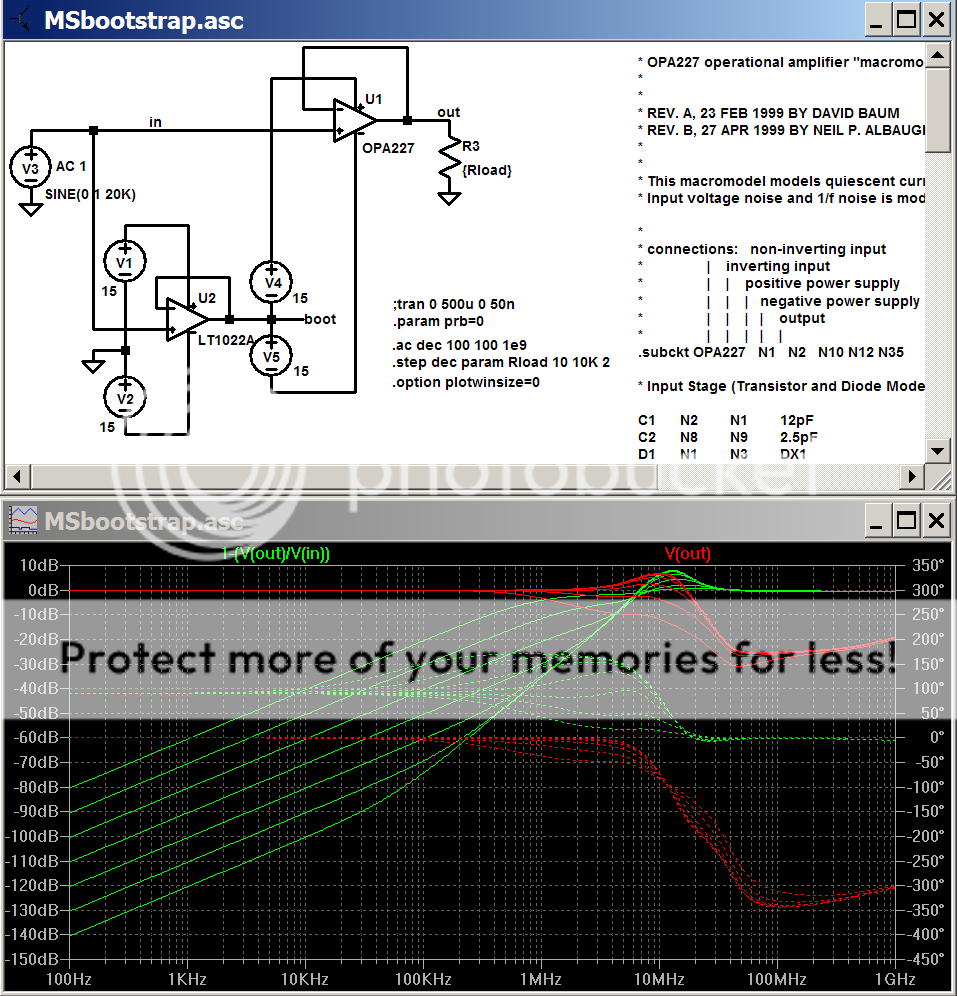
(captured screen shot pasted into "paint" program, cropped, saved as .png, hosted on free photobucket.com account)
Lt Spice schematic .asc file faked into diyaudio by adding .txt extension - just rename without the .txt
Attachments
mikeks said:Similarly, your modification provides us with a double-pole characteristic for the major loop, while delivering the equivalent triple-pole compensated characteristic in respect of the second and output stages; the later is clearly unstable.
If you look at the plots though, the instability of the "Mike" loop gain(**) of the last one I posted is due only to the peaking at 30 MHz of the output stage. The lower frequency phase margin is well behaved. And the one from my amp, for which the "Mike" loop gain looks like first order over much of the frequency range, is not unstable at all. The biggest difference between these two circuits is that in the well-behaved one, both the VAS and its constant-current load are cascoded. Also, the first active device in my output stage is a MOSFET. This all adds up to a very high impedance at the node where the VAS and output stage come together. The two-pole comp seems to behave in the most predictable way when the total impedance at this node is as high as possible. So I am going to try cascoding the VAS and its constant-current load in the all-bipolar circuit to see if the "Mike" loop gain becomes less quirky. Of course, I'll remove the EF from the VAS in this case.
I think it's safe to say that neither of us has a rigorous mathematical model for what's going on here, so experimentation in this way seems appropriate.
...the series combination of the three capacitors in your arrangement must be identical to those selected for the equivalent DPC network if the forward-path's unity gain frequency is to remain unchanged.
Totally agree on that one.
I'll be offline for the rest of the evening tonight. Tomorrow I need to order the rest of my HV regulator parts so it may be a bit before I post those results. This is becoming more time-consuming than I had bargained for.
(**) The "Mike" loop gain is calculated by having the loop gain probe right at the output of the output stage.
Bob Cordell said:
... One thing that I need to point out is in regard to my level of conservatism in applying DPC. I am not comfortable with the phase margin dipping below about 35-40 degrees anywhere in the rolloff slope. In other words, I'm saying that if the gain were to decrease anywhere by an arbitrary amount, there would still be at least 30-40 degrees of phase margin at the resulting gain crossover point. This is why I prefer to view this form of compensation as an approximation to a constant rolloff slope of greater than 6 dB/octave.
Bob
Bode's "maximum feedback" design critieria is I believe more relevant to tube amps:
jcx said:Bode's maximum feedback loop gain curve’s slope is set to give a fixed minimum phase margin at any frequency - 30-60 degrees is the typical recommendation
this is to assure that for nonlinear operation that reduces the effective amplifier gain without much affecting the phase shift the feedback won't cause the reduced gain amplifier to oscillate/behave badly - tube amps are apparently especially problematic since their gain sweeps from zero to the operating gain slowly each time the amp is powered up and the phase shift is largely determined by parasitic C that doesn’t change too much with bias point
with 2 pole compensation you have 180 degrees phase shift in the feedback network = zero (or negative if the amp contributes any phase shift) phase margin over the region where the loop gain slope is near 40dB/decade –this region of the Nyquist diagram plot “pokes up” above the 180 phase axis and as the amp gain grows radially from 0 to the final gain locus there is an intermediate gain region where the magnitude 1, 180 degree point is encircled by the gain locus
for ss amps the turn on transient can be much faster and more complicated - and semiconductor junction C is 1st order sensitive to bias point - if the operating bias point is reached much faster than a cycle of the potential feedback oscillation frequency there may not be a problem
but nonlinear operation such as clipping or slew rate limiting reduces the effective gain of the amplifier viewed at the fundamental frequency of the input frequency and the amplifier can show jump resonance (= “hysteric” clipping, you have to reduce the input level well below the initial clipping level for the amp to return to normal linear operation) or even self sustaining large signal oscillation that is triggered by input in the frequency region of negative phase margin even though the linear stability margins are fine at the much higher loop gain intercept frequency
despite the potential problems 2-pole compensation seems to work in practical amplifiers (the region of pure 2-pole slope shouldn’t be large in audio amps so the full 180 degree feedback phase shift isn’t usually reached) – but you really need to address the potential clipping behavior if you try to go even further – ever see a “3 pole” loop gain amplifier?
Cherry makes this point in his discussion of his nested differentiating feedback loops which are "conditionally stable" by Bode's criteria
As a speculation I would guess some of the practical determinants in successful amp topologies are driven by the nonlinear /clipping recovery behavior - after all linear theory points to maximizing global loop gain as the most "efficient" approach for reducing distortion with negative feedback, so why look elsewhere?
the choices of local vs global feedback (and compensation) have to satisfy linear stability but there is also this far more complex nonlinear performance that is seldom discussed - probably the preference for miller-dominant pole compensation + unity gain output stages is driven by this
The relative dominance of audio power amps by only a few fundamental topologies probably reflects in part the dismissal of those that have great linear performance but self destruct from these nonlinear oscillations/latch up effects at the least provocation
Bob’s input clipping (and input bandwidth limiting = slew rate limiting) may be useful for expanding the range of low distortion audio power amplifier topologies that could be used - although conditionally stable designs likely will require complicated internal current/saturation/gain limiting "nonlinear compensation" circuitry for safe operation
While Cherry’s ndf amplifiers don’t seem to have carried the market, Halcro’s designs which also play in the “conditional stability” end of high feedback design do seem to have some success
- Home
- Amplifiers
- Solid State
- Bob Cordell Interview: Negative Feedback