Some Ph.D 'over there' (let's call her Ophelia) has tried to analyze TMC by means of old school pen and paper math. Here follows a few of Ophelia's conclusions:
> In fact, the phase dip is not cancelled in any way (that would actually be impossible for a second order system)
> but because the remaining gain available to wrap (and linearize) the VAS is greatly reduced (and hence so is the phase dip).
Indeed, that would be impossible for a second order system. The real reason for the absence of a phase dip lies in the fact that TMC is NOT a second order system. The difference between TPC and TMC is that TPC acts on the whole signal of the VAS output, while TMC acts on the difference between OPS output and VAS output, i.e. the error signal from the OPS.
So, one might say that only the error signal is "TPCed". As this signal is only a small fraction of the whole signal, the increase in order (due to TMC) is also a small fraction compared to a 2nd order system like TPC. If, for example, the error signal is 2% (which is equivalent to a OPS gain of 0.98), then the 'order' is 1.02. That is the reason why there is (almost) no phase dip and overshoot. (This also means that the lower the OPS gain, the more phase dip and overshoot. )
> On the flip side, TMC extra loads the input stage, with the equivalent lead-lag compensation network Miller reflection. For identical global amp
> results, this may require a beefier input stage (more current, more degeneration, etc...) compared to simple Miller or TPC compensation.

Is that So? Let's have a look at the (simmed) output current of the input stage for a typical blameless amp with respectively Miller, TPC and TMC compensation. f=100kHz and Vi=1V
Miller: 261.0nA
TPC: 265.9nA
TMC: 260.5nA
So TMC results in the lowest IPS output current of all of the three compensation schemes. Needless to say that I've no trouble with this alleged 'flip side'. 😀
Bottom line: Never trust pen and paper math. Always verify the results by means of simulation.
Cheers,
Edmond.
Hi again Edmond, I'm not sure I follow, but it seems counter intuitive to me for all three Miller, TPC and TMC schemas to have the same VAS input impedance (and therefore equally load the input stage). Perhaps in your results it is the phase of the input current that makes a significant difference for the input impedance? Anyway, could you please provide a reference/link for this 'over there' analysis?
Hi again Edmond, I'm not sure I follow, but it seems counter intuitive to me for all three Miller, TPC and TMC schemas to have the same VAS input impedance (and therefore equally load the input stage).
Hi YWN,
This is because the Miller cap (C1) 'sees' (almost) the same voltage in all three cases.
Perhaps in your results it is the phase of the input current that makes a significant difference for the input impedance?
No.
Anyway, could you please provide a reference/link for this 'over there' analysis?
DIY Audio Engineering » General Electronics Design » General Design - Theory and Practice » To TMC or not to TMC, posted on November 25, 2010
Cheers,
E.
Some Ph.D 'over there' (let's call her Ophelia) has tried to analyze TMC by means of old school pen and paper math. [snip]Edmond.
Edmond,
I gather that 'Ophelia' has no opportunity to explain 'her' reasoning here? Personally, it find it not 'nice' to try to score your points this way.
But I am known to be oldfashioned...
jan didden
I have no opportunity to put my reply 'over there'.
Besides, maybe I've very good reasons to be not that 'nice'.
Besides, maybe I've very good reasons to be not that 'nice'.
if DIY-audioengineering won't award posting rights then how else can the misinformation be discussed?
It's even worse, they won't let you read attachments. So no diagrams to confirm what is being discussed.
It's even worse, they won't let you read attachments. So no diagrams to confirm what is being discussed.
Hi YWN,
This is because the Miller cap (C1) 'sees' (almost) the same voltage in all three cases.
Cheers,
E.
Hi Edmond, sorry for being again a PITA, but I don't understand what you are saying here. Could you post the schematic/method you are using to determine the VAS input impedance?I took a look to the 'other place' but unfortunately I can't see the attachments, so I have no idea what is the guy trying to do.
TMC
Hi YWN,
For a schematic please look here: http://www.diyaudio.com/forums/soli...erview-negative-feedback-311.html#post2367976
but tie the left side of R1 to 'out' and omit R2 & C3.
I didn't look at the input impedance of the VAS. Instead, I looked at the AC output current of the input stage, as this was what Ophelia was whining about:
this may require a beefier input stage (more current, more degeneration, etc...)
which is simply not true.
Cheers,
E.
Hi Edmond, I'm afraid I still don't get it; where is the input signal, is the global feedback loop open or closed? I don't see how the input stage output current (or the VAS input current) could be the same, if the VAS input impedances are different. But then I see you have little patience with reconciling and explaining different views of the same physical reality and prefer to deal with things in a rather confrontational manner. So I'll leave it here and eventually try to draw my own conclusions. Thank you for your help, and I apologize again for intruding in a discussion that is obviously well over my head.
the link took me to post 3251. Where should it take me?For a schematic please look here: http://www.diyaudio.com/forums/soli...erview-negative-feedback-311.html#post2367976
the link took me to post 3251. Where should it take me?
The links do not appear to be working correctly. It appears to be a site problem, because the links appear to be pointing directly to a particular post. I've seen this problem before. Perhaps a moderator could look into it.
Hi Edmond, I'm afraid I still don't get it; where is the input signal,
The input signal is delivered to node 'IN' by V1. Can't you read a schematic?
is the global feedback loop open or closed?
It's closed. Can't you read a schematic?
I don't see how the input stage output current (or the VAS input current) could be the same, if the VAS input impedances are different.
The VAS input impedances are NOT different, that is, in case of the original TMC amp.
However, Ophelia (Ph.D) has transformed the TMC stuff into something else, which is not equivalent to the original. As a result, she has drawn the wrong conclusions.
But then I see you have little patience with reconciling and explaining different views of the same physical reality
I don't have trouble with different views as long as we are talking about the same physical reality.
and prefer to deal with things in a rather confrontational manner. So I'll leave it here and eventually try to draw my own conclusions. Thank you for your help, and I apologize again for intruding in a discussion that is obviously well over my head.
What about putting me on your ignore list?
TMC
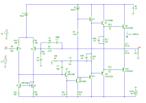
Here's a copy of the schematic (notice: a TPC amp):
the link took me to post 3251. Where should it take me?
Here's a copy of the schematic (notice: a TPC amp):
Attachments
Post 3105.the link took me to post 3251. Where should it take me?
[ot] I notice you keep getting lost following links. Maybe it's to do with number of posts displayed per page. I use "forum default" which is 10.[/ot]
yes, certainly to do with page default and the way posters choose their link label.
If the poster goes to the post number and right clicks then the option comes up to link directly to the correct post (copy link location). I use Firefox.
If the poster goes to the post number and right clicks then the option comes up to link directly to the correct post (copy link location). I use Firefox.
Last edited:
Bottom line: Never trust pen and paper math. Always verify the results by means of simulation.
Cheers,
Edmond.
Bottom line: ALWAYS use pen and paper FIRST, trust the math, THEN you can do the simulation.
Cheers
S
Here's a copy of the schematic (notice: a TPC amp):
Hi Edmond,
Your posted schematic reminded me of another thing that might deserve some discussion - that is the use of the speedup capacitor, C6 in your schematic.
I'll be the Devil's advocate here and say that I do not trust the use of speedup capacitors. They are a crutch for designs where the idle bias of the drivers was not high enough in the first place to adequately quickly turn off the output transistors under conditions of high rate of change of output current. They may make designers complacent in that they may improve static THD-20. Present company excluded, of course.
However, to be effective, it seems that if you do the calculations the speedup capacitor needs to be moderately large to thoroughly do the job of pulling out base charge. If they are large, and they have had to do that job, then they will necessarily have aquired a charge. The time constant of the capacitor against the emitter bias resistor may be long enough for the remant effects of that charge to persist over several cycles, possibly leading to an upset bias condition after the event that required the presence of the speedup capacitor.
On general principle, we always have to be very careful when we combine a capacitor (or other charge-storage device) with a nonlinearity (the emitter-base junctions of the drivers). What say you to this food for thought. I seem to recall touching on this in chapter 10 of my book.
I like drivers that really suck without benefit of a speedup capacitor 🙂. The price to be paid is running the drivers hot. I have never used a speedup capacitor in any of my designs.
Cheers,
Bob
speedup cap.
Hi Bod,
I fully agree with all these points. As a matter of fact I really hate that speedup cap, perhaps even more than you do. I only dropped that schematic (with that ***** cap) for the sake of simplicity, to demonstrate the principle of TMC and to avoid confusion and/or a debate on other topics.
Perhaps you've overlooked it (never mind, no one can read read all posts), but here you can see that I'm fully aware of the pitfalls of that cap and how to overcome the disadvantages: http://www.diyaudio.com/forums/solid-state/174218-rebirth-phoenix-3.html#post2336489 by putting two TT-diodes between the bases of the OP trannies
See also: http://www.diyaudio.com/forums/solid-state/174218-rebirth-phoenix-2.html#post2334955 for more details. That was a very clever idea. Again, thank you!
Of course you can do it that way, but for those who like 'green' amps, one can avoid running them hot by using two class-AB totem drivers: one for the 'top' OP device(s) and a separate one for the 'bottom' OP device(s). See for the basic idea: http://www.diyaudio.com/forums/soli...terview-negative-feedback-92.html#post1229115 Q9, Q10, Q12 & Q13 (D2 & D3 are LEDs).
Cheers,
Edmond.
Hi Edmond,
Your posted schematic reminded me of another thing that might deserve some discussion - that is the use of the speedup capacitor, C6 in your schematic.
I'll be the Devil's advocate here and say that I do not trust the use of speedup capacitors. They are a crutch for designs where the idle bias of the drivers was not high enough in the first place to adequately quickly turn off the output transistors under conditions of high rate of change of output current. They may make designers complacent in that they may improve static THD-20. Present company excluded, of course.
However, to be effective, it seems that if you do the calculations the speedup capacitor needs to be moderately large to thoroughly do the job of pulling out base charge. If they are large, and they have had to do that job, then they will necessarily have aquired a charge. The time constant of the capacitor against the emitter bias resistor may be long enough for the remant effects of that charge to persist over several cycles, possibly leading to an upset bias condition after the event that required the presence of the speedup capacitor.
Hi Bod,
I fully agree with all these points. As a matter of fact I really hate that speedup cap, perhaps even more than you do. I only dropped that schematic (with that ***** cap) for the sake of simplicity, to demonstrate the principle of TMC and to avoid confusion and/or a debate on other topics.
Perhaps you've overlooked it (never mind, no one can read read all posts), but here you can see that I'm fully aware of the pitfalls of that cap and how to overcome the disadvantages: http://www.diyaudio.com/forums/solid-state/174218-rebirth-phoenix-3.html#post2336489 by putting two TT-diodes between the bases of the OP trannies
See also: http://www.diyaudio.com/forums/solid-state/174218-rebirth-phoenix-2.html#post2334955 for more details. That was a very clever idea. Again, thank you!
On general principle, we always have to be very careful when we combine a capacitor (or other charge-storage device) with a nonlinearity (the emitter-base junctions of the drivers). What say you to this food for thought. I seem to recall touching on this in chapter 10 of my book.
I like drivers that really suck without benefit of a speedup capacitor 🙂. The price to be paid is running the drivers hot. I have never used a speedup capacitor in any of my designs.
Cheers,
Bob
Of course you can do it that way, but for those who like 'green' amps, one can avoid running them hot by using two class-AB totem drivers: one for the 'top' OP device(s) and a separate one for the 'bottom' OP device(s). See for the basic idea: http://www.diyaudio.com/forums/soli...terview-negative-feedback-92.html#post1229115 Q9, Q10, Q12 & Q13 (D2 & D3 are LEDs).
Cheers,
Edmond.
Bottom line: ALWAYS use pen and paper FIRST, trust the math, THEN you can do the simulation.
Cheers
S
In some way it reminds me of that old-fashioned accountant who got a computer from boss. As he didn't trust the machine, everyday he checked the results by hand. 😛
- Home
- Amplifiers
- Solid State
- Bob Cordell Interview: Negative Feedback