mikeks said:.....no pots. or sundry tuning required.
Actually, Bob was absolutely right: given that, of necessity, the gain around the loop defined by summers S1 and S2 (with respect to the extracted error ''e'') must be exactly unity for complete error cancellation, it follows that in practice some measure of pot. tuning may be required to extract optimal performance.
This, clearly, also obtains for Yokoyama's arrangement.
It is of interest that while summers S1 and S2 are implemented by a single transistor in Bob's amplifier, Yokoyama's figure 2 uses two stages: an emitter coupled pair for S1, and the current mirror/TIS collector for S2.
I dare say the division of circuit functions in the later arrangement affords superior linearity, accuracy and precision with respect to the former.
Alas, the statement below extracted from this post cannot be correct.
This is because (as indicated in post#721 above) the gain around the loop defined by S1 and S2 must be unity, at least nominally, for error cancellation to occur.
This explains the presence of resistive second stage collector loads ''21'' and ''22'' in Yokoyama.
The low values used probably explains why Yokoyama did not use Miller compensation: the minor loop capacitor required in these circumstances would need to be inordinately large.
Moreover, these resistors are a veritable PITA, as they generate significant distortion in the second stage; this is probably why Yokoyama's THD+N results are significantly inferior to Bob's arrangement.
mikeks said:This eliminates the low impedance drive required by the Hawksford scheme to properly and resistively define the collector loads in his error amplifiers.
This is because (as indicated in post#721 above) the gain around the loop defined by S1 and S2 must be unity, at least nominally, for error cancellation to occur.
This explains the presence of resistive second stage collector loads ''21'' and ''22'' in Yokoyama.
The low values used probably explains why Yokoyama did not use Miller compensation: the minor loop capacitor required in these circumstances would need to be inordinately large.
Moreover, these resistors are a veritable PITA, as they generate significant distortion in the second stage; this is probably why Yokoyama's THD+N results are significantly inferior to Bob's arrangement.

andy_c said:
Thanks Bob. Lots of things have changed for the better as far as usability of SPICE and availability of models are concerned. Writing computer programs back then was a complete PITA. Heck, my original FORTRAN class used punch cards. That was awful. It's amazing how far computer-aided design techniques have come since then.
andy_c said:
Wow, think of the probability of that. That's like 1 divided by the number of atoms in the universe or something 🙂.
ROFL!
I believe we used the IBM 360 also. The computer center was really crowded, so even if I waited until midnight, I'd still have to wait in line for punch card machines. Then I'd punch the cards and give them to some guy in a room that was like a big closet. Then the next morning I'd find out my program didn't compile. After that, I swore I'd never touch a computer again. And I didn't for 10 years until I built a 286 clone.
You too? You must be of my generation. I learned with Fortran G and WATFOR on an IBM 360 - with punch cards, of course. It was heaven when I graduated to an IBM 370-168 at Bell labs. BIG IRON!! But then there was the Intel 8008 with 1kbit static rams, programmed in Intel assembly language.
Bob
Bob Cordell said:First, notice the collector load resistors to ground on the output of the VAS. This is necessary to establish a known gain for the injected error signal to work with. The need to drive this load taxes the VAS and may cause it to have higher distortion.
Bob
True!

just ran andy_c's sim,
it needs the spice directive line:
.option plotwinsize=0
or turn off waveform compression in the tools menu
another point is that Vsource drive is not nearly the right input condition, the error amp is driven from the cascoded VAS/TIS high impedance current output, with the compensation C4, R13 in feedback around the input defining a frequency dependent source impedance for the error correction stage
any thoughts on a good approximation for the combined gm from diff input to error amp input? With some reasonable # for the NDP5564 gm at 2mA? I could patch up a g_source front end for this sim
Bob Cordell said:You too? You must be of my generation. I learned with Fortran G and WATFOR on an IBM 360 - with punch cards, of course. It was heaven when I graduated to an IBM 370-168 at Bell labs. BIG IRON!! But then there was the Intel 8008 with 1kbit static rams, programmed in Intel assembly language.
Probably close. I turned 50 this year. I'm the guy that was asking questions about your error correction amp article at the RMAF amplifier design Q&A.
The Fortran book we had was "Fortran IV with WATFOR and WATFIV". To this day I still do not know WATTF either WATFOR or WATFIV was 🙂. I did find out later that they were from Watcom, which was apparently associated with the University of Waterloo at Ontario. There is some history of Watcom here. i got into C and C++ in the late '80s and worked for a simulator company for 5 years or so until just recently.
jcx said:just ran andy_c's sim,
it needs the spice directive line:
.option plotwinsize=0
or turn off waveform compression in the tools menu
Ah. thanks for catching that. It was an old sim that I fixed up. I used to disable waveform compression in the dialogs until I later found out about .options plotwinsize=0. I should have caught that.
BTW, in speaking to Bob at the RMAF, I found that he measured the distortion of the output stage by itself by hooking up the global feedback loop to the VAS output. So the zero impedance should represent that condition adequately. Otherwise, some pretty intimate knowledge would be required to get the right impedance for the case when the loop is closed around the overall amp.
changed most part designators to the jaes paper #s
added a voltage dependent current source input stage "macromodel"
it runs, still needs andy's zip files
"Total Harmonic Distortion: 0.000418%"
probably will need the loopgain probe to tell much about the nested loops
more guidance on input diff pair gm is still needed
added a voltage dependent current source input stage "macromodel"
it runs, still needs andy's zip files
"Total Harmonic Distortion: 0.000418%"
probably will need the loopgain probe to tell much about the nested loops
more guidance on input diff pair gm is still needed
Attachments
Hi, Bob Cordell,
If the output stage is bipolar, low biased classAB. Will putting Hawksford EC give huge improvement as if it was implemented in Mosfet output stage?
If the output stage is bipolar, low biased classAB. Will putting Hawksford EC give huge improvement as if it was implemented in Mosfet output stage?
lumanauw said:Hi, Bob Cordell,
If the output stage is bipolar, low biased classAB. Will putting Hawksford EC give huge improvement as if it was implemented in Mosfet output stage?
Interesting question David. I have a related question: Bob, your design integrates H.ec as well as strong global feedback. If you would disconnect the H.ec, how much would the performance change? I understand that H.ec comes almost free the way you inplemented it, but it would be of interest to know.
Jan Didden
Hi, Janneman,
May I add another one? 😀 How about a non-global feedback power amp, but have Hawksford EC in output stage (Like Steven's).
How does this compare to global feedback power amp+Hawksford EC (like Bob Cordell's)?
This is Steven's design :
http://www.diyaudio.com/forums/showthread.php?postid=330446#post330446
lumanauw said:Hi, Janneman,
May I add another one? 😀 How about a non-global feedback power amp, but have Hawksford EC in output stage (Like Steven's).
How does this compare to global feedback power amp+Hawksford EC (like Bob Cordell's)?
This is Steven's design :
http://www.diyaudio.com/forums/showthread.php?postid=330446#post330446
In my experience, a global nfb amplifier will measure better than non-global nfb amp with H.ec. But that is based on just one or two trials and I would be interested in Bob's views.
Jan Didden
Folks, i think Hawksford (and Cordell) were preceded by Mr Henri Pichal as far back (at least!) as 1972!
Andy_c wrote:
How about some measurements to help understand how the output stage works? For example,
- gain and phase vs f (eg: 1kHz to 100MHz), input to output with 8-ohm load
- output Z vs f, with Vin (ac) = 0
- input Z vs f, with Zout = 8-ohm
and, feedback loop gain and phase vs f.
To keep it simple, Vin and Vout dc=0.
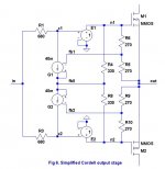
I've created a simplified diagram (Fig 6) of the output stage to help describe the principle of how it works. The diagram omits biasing and frequency compensation.
You can see it is two mirrored circuits, each being a Hawksford EC. Looking at the positive (top) half first, the voltaged controlled current source, G1, measures the output FET gain error. The error signal is a current and this current, combined with R1, subtracts the error from the input voltage. So in fig 11 of Bob's paper, G1 does the job of S1 and R1 does the job of S2. The modified input signal, x1, is then buffered by E1 before becoming the gate drive voltage n1.
The gain equations are:
v(x1) = v(in) - gm1.[v(fb0) - v(fb1)].R1
v(x2) = v(in) + gm2.[v(fb0) - v(fb 2)].R3
v(n1) = v(x1), v(n2) = v(x2)
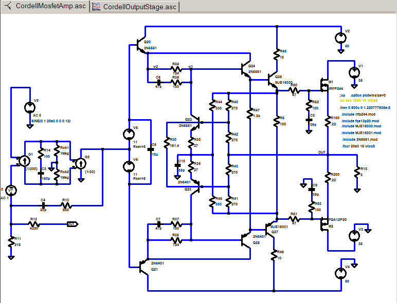
Thanks Andy.Okay, here is a sim of Bob's output stage.
How about some measurements to help understand how the output stage works? For example,
- gain and phase vs f (eg: 1kHz to 100MHz), input to output with 8-ohm load
- output Z vs f, with Vin (ac) = 0
- input Z vs f, with Zout = 8-ohm
and, feedback loop gain and phase vs f.
To keep it simple, Vin and Vout dc=0.
I've created a simplified diagram (Fig 6) of the output stage to help describe the principle of how it works. The diagram omits biasing and frequency compensation.
You can see it is two mirrored circuits, each being a Hawksford EC. Looking at the positive (top) half first, the voltaged controlled current source, G1, measures the output FET gain error. The error signal is a current and this current, combined with R1, subtracts the error from the input voltage. So in fig 11 of Bob's paper, G1 does the job of S1 and R1 does the job of S2. The modified input signal, x1, is then buffered by E1 before becoming the gate drive voltage n1.
The gain equations are:
v(x1) = v(in) - gm1.[v(fb0) - v(fb1)].R1
v(x2) = v(in) + gm2.[v(fb0) - v(fb 2)].R3
v(n1) = v(x1), v(n2) = v(x2)
Attachments
jcx said:changed most part designators to the jaes paper #s
added a voltage dependent current source input stage "macromodel"
it runs, still needs andy's zip files
"Total Harmonic Distortion: 0.000418%"
probably will need the loopgain probe to tell much about the nested loops
more guidance on input diff pair gm is still needed
Hi JCX
I run your netlist, but obtained a ''multiple instances of flag'' error.
...am i doing something wrong?
mikeks said:Alas, the statement below extracted from this post cannot be correct.
This is because (as indicated in post#721 above) the gain around the loop defined by S1 and S2 must be unity, at least nominally, for error cancellation to occur.
This explains the presence of resistive second stage collector loads ''21'' and ''22'' in Yokoyama.
The low values used probably explains why Yokoyama did not use Miller compensation: the minor loop capacitor required in these circumstances would need to be inordinately large.
Moreover, these resistors are a veritable PITA, as they generate significant distortion in the second stage; this is probably why Yokoyama's THD+N results are significantly inferior to Bob's arrangement.
Not entirely true as the collector resistors are connected to the output rather than ground.
Be that as it may, distortion is still compromised relative to Cordell.
Apologies, I got the signs wrong on the gain equations:
v(x1) = v(in) + gm1.[v(fb0) - v(fb1)].R1
v(x2) = v(in) - gm2.[v(fb0) - v(fb 2)].R3
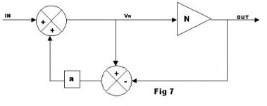
How do we calculate "correction" power? To find out, refer first to Hawksford's model in Fig 7. The idea is that Vn changes to correct error in N. In other words, Vn should change in response to a change in Vout. We make Vin = 0 for this.
In fig. 7,
Vn = a.(Vn - Vout)
Vn.(1 - a) = -a.Vout
Vn/Vout = -a/(1 - a)
When a = 1, Vn changes infinitely and out of phase with Vo. This is the maximum correction condition. It should be out of phase as it is trying to "correct" Vo. But a practical circuit will not work with infinite gain.
Next installment...how much "correction" power does Bob's circuit provide?
v(x1) = v(in) + gm1.[v(fb0) - v(fb1)].R1
v(x2) = v(in) - gm2.[v(fb0) - v(fb 2)].R3
How do we calculate "correction" power? To find out, refer first to Hawksford's model in Fig 7. The idea is that Vn changes to correct error in N. In other words, Vn should change in response to a change in Vout. We make Vin = 0 for this.
In fig. 7,
Vn = a.(Vn - Vout)
Vn.(1 - a) = -a.Vout
Vn/Vout = -a/(1 - a)
When a = 1, Vn changes infinitely and out of phase with Vo. This is the maximum correction condition. It should be out of phase as it is trying to "correct" Vo. But a practical circuit will not work with infinite gain.
Next installment...how much "correction" power does Bob's circuit provide?
Attachments
Hi, Traderbam,
Could this be called EC?
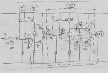
I draw a 3 stages power amp (differential, VAS, output stage).
The main function is :
R1-R2 is input resistors. R3-R4 is voltage divider (that set the whole amp gain). T1-T2 (block I) is main differential. T3 is main VAS (block II). T4-T5 is buffer.
The output stage (block III) is another 3 stages amp, consist of differential (T6-T7), VAS (T8) and output stage (T9-T10-T11-T12)
Can T6-T7-T8-T9-T10-T11-T12 considered an output stage with EC capability? The purpose of block III is only to set G=1 (setting point A = point B, no voltage divider at base of T7) ?
Could this be called EC?
I draw a 3 stages power amp (differential, VAS, output stage).
The main function is :
R1-R2 is input resistors. R3-R4 is voltage divider (that set the whole amp gain). T1-T2 (block I) is main differential. T3 is main VAS (block II). T4-T5 is buffer.
The output stage (block III) is another 3 stages amp, consist of differential (T6-T7), VAS (T8) and output stage (T9-T10-T11-T12)
Can T6-T7-T8-T9-T10-T11-T12 considered an output stage with EC capability? The purpose of block III is only to set G=1 (setting point A = point B, no voltage divider at base of T7) ?
Attachments
Hi lumanauw,
in my opinion, yes. What you have drawn is an output stage with unity-gain NFB around it. Then you've added a front end with voltage gain and put global NFB around the whole thing. In gain structure, this is the same type as Bob's amplifier.
I suppose this could be called various things...
1) An amplifier with output "EC" and global NFB (similar to Bob's)
2) A nested feedback amplifier
3) A NFB amplifier wrapped around a NFB amplifier
I notice the term "error correction" seems to be a popular replacement for the term "unity-gain feedback" when applied to an output stage. I see no reason to restrict an output stage to unity gain. You can choose to apportion the gains between the inner and outer amps to suit your purpose.
Brian
- Home
- Amplifiers
- Solid State
- Bob Cordell Interview: Error Correction