Bob Cordell said:
In practice, I believe it is better sonically to over-bias (Class AAB) and take some gm doubling, since in reality it is difficult to manage that small optimum bipolar bias current in the face of large current changes and thermal variations that cannot be properly tracked (because the thermal time constant of the output transistor die is much shorter than that of the heatsink, just for starters).
I believe it is even better to load a source (or/and emitter) follower by a U/I converter so there will be no way to generate any crossover distortions, and current consumed by the output stage will only be twice on higher peaks against iddle current. However, there will be very small 2'nd order harmonics generated, unfortunately higher on top frequency end, but I don't see how sonicaly better amplification may be done using available today active elements.
ingrast said:If the AES review panel finds merits for publication, then full details will be available there.
Hi Rodolfo,
Best of luck with getting your paper published, and I look forward to reading it!
andy_c said:
Hi Rodolfo,
Best of luck with getting your paper published, and I look forward to reading it!
Thanks for the good wishes Andy !!
Rodolfo
ingrast said:
In fact it works, and I have test amplifiers measured (better than 0.001% THD, beyond my current measurement capabilites) and working now for hundreds of accumulated hours without problems whatsoever.
The underlying theoretical approach to understand how EC in a generalized form relates to GNF, simulation results and prototype results, was condensed in a paper draft Jan reviewed well over a year ago as well as the faculty at the Institute of Electrical Engineering here in Montevideo.
The paper draft has been reviewed also by Mr. Andres Mayo, VP Latin America, AES, who found merits enough for submission to review for eventual publication in the JAES.
I do not know for sure at this time whether partial or full disclosure is allowed being the paper under review, so I cannot provide more details for the time being, something I hope will not hold for long. If the AES review panel finds merits for publication, then full details will be available there.
As is usually the case, I applied for a patent based not really on the topology itself - pretty much prior art at this time - but on the prerequisites for its succesfull application, which are the core of the draft.
Rodolfo
Thanks for the update. Is this different than what Jan described in his preprint #4597? Can you tell us more about the amplifier you have built to demonstrate it? For example, is it MOSFET or bipolar?
If I understand correctly, your design was written up and submitted for publication in the JAES, as opposed to being submitted for presentation at a convention? How long ago was it put in the JAES review pipeline?
Thanks and good luck.
Bob
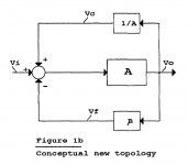
Sorry about this Rodolfo but I feel I should point something out before you publish. Just in case. 🙂 I have thought of a possible disadvantage of Jan's technique over conventional NFB in a practical circuit.
In a normal NFB loop the OL gain is generated linearly before the device being "corrected". In Hawksford's system the forward gain is generated by a positive loop before the distorting device. However, in Jan's topology the forward gain is generated by positive feedback taken AFTER the distorting device.
This matters because any error appearing at the output, which is not conjugated away by the 1/A block, is fed back regeneratively. Distortion is added positively to the input summer. In other words the OL forward gain is polluted by the output distortion.
You need to do the maths, but I suspect that for the same OL gain, a conventional NFB loop will show significantly better distortion rejection and rejection of external noise at the output.
Just thought you ought to check this out if you haven't already considered it.
Brian
Bob Cordell said:
Thanks for the update. Is this different than what Jan described in his preprint #4597? Can you tell us more about the amplifier you have built to demonstrate it? For example, is it MOSFET or bipolar?
Bob:
As said previously, the topology is the same - though I was not aware at the time of starting with this 2 years back -, but the novelty is basically in understanding the summing node role and requirements.
The amplifier is basically a CFP with MOS output transistors, while the summing node is an OpAmp. The CFP is actually the plant. In the prototype version I was mostly concerned with the EC concept so did not go to great lengths with regards to biasing, with the result of a quite hot concotion!! The preproduction module - the ones I listen to regularly - have active bias control I described previously in the Ever made a MOSFET CFP/Sziklai that works? thread.
If I understand correctly, your design was written up and submitted for publication in the JAES, as opposed to being submitted for presentation at a convention? How long ago was it put in the JAES review pipeline?
Thanks and good luck.
Bob
I do not have right now (not at home) the exact date, but was asked for confirmation of submission I guess about 3-4 weeks ago. I was advised then the process could take anywhere from 3 - 4 months.
I must confess I was tempted to contact you in this regard when this thread started - it was after the submission -, but the fact you belong to the AES review board refrained me (you are also cited in the references), on the grounds it could be taken as an attempt outside the regular channels.
Thanks for the good wishes !!
Rodolfo
traderbam said:Jan,
Your idea is very creative.[snip]
Thank you

traderbam said:[snip]I think it will be very hard to make it work for a practical gain element A that has phase shift and potentially even time delay. The positive feedback element 1/A would have to have corresponding phase lead and time reversal.
And if you could make a perfect 1/A element, you might as well use it as a pre-distortion block ahead of A. Then you have a zero distortion OL system without any feedback, which would be better.
I guess a practical system will necessarily operate with the positive feedback gain being 1/C where C>A. The question is about whether it is better to implement a particular system with a positive feedback loop to generate the OL gain or whether it is better to put a gain block in series with A.
This is one reason why I looked to another way to get high linearity without global nfb. What you mention is the reason they call this a 'null network' : the exact cancellation of the error is easy to do for a specific point in the transfer function but quite difficult for 20Hz-20kHz and 1mV to 20V. You can, but the circuit complexity rapidly increases to the point that it is more involved than 'simple' global nfb.
To be sure, H.ec is also a null network, but I have better experiences with it. That is one reason why I think it is not really equivalent to your fig 2 way above. But I can't pinpoint it. Yet.
Jan Didden
traderbam said:......
In a normal NFB loop the OL gain is generated linearly before the device being "corrected". In Hawksford's system the forward gain is generated by a positive loop before the distorting device. However, in Jan's topology the forward gain is generated by positive feedback taken AFTER the distorting device.
.....
Brian
Brian:
I am not quite sure about what you are talking for I do not have right now at hand Jan's schematics. Anyway the concept is basically to start with a non-ideal plant, and to feed back as error the difference among its input and its (scaled down) output. It is assumed the summing node is at least perfectly linear, though this is not the only constraint and this is the study subject.
Rodolfo
Rodolfo,
To understand you have to think of the circuit as a high NFB system whose forward gain is derived from the 1/A loop. The 1/A loop feeds the output back to the input positively.
In negative feedback the output error is subtracted from the input and this reduces the error at the output (if the system is stable). If the feedback is positive the output error will be increased.
Since the forward gain for this system is created by positive feedback, any error at the output will be bigger than it would have been if the forward gain had been generated cleanly.
I suspect this will also show up as a higher output Z than a conventional NFB system, when both have identical forward gain.
Brian
Attachments
Please take a look at page-14 of this one:
http://www.yorkville.com/downloads/servman/smap4040.pdf
With a very very very small modification it could be transformed in error correction!
http://www.yorkville.com/downloads/servman/smap4040.pdf
With a very very very small modification it could be transformed in error correction!
traderbam said:Rodolfo,
To understand you have to think of the circuit as a high NFB system ....
Brian
Brian:
If you go on to Fig. 2b in Jan's presentation, you will notice the 1/A branch is relocated (and 1/A dropped) to the summing node's output. This is error correction it its pure form, and system gain is set only by 1/beta.
Rodolfo
TOINO said:Please take a look at page-14 of this one:
http://www.yorkville.com/downloads/servman/smap4040.pdf
With a very very very small modification it could be transformed in error correction!
In most cases it is possible with a small modification to convert to EC, the catch is to really get a better result.
Rodolfo
Ok I see.
Fig 2b is not the same system as fig 1b. Jan has put a positive feedback loop ahead of A to generate the forward gain. Yes, that ought to reduce the problem I spotted in fig 1b. I should have read ahead, sorry.
Brian
Fig 2b is not the same system as fig 1b. Jan has put a positive feedback loop ahead of A to generate the forward gain. Yes, that ought to reduce the problem I spotted in fig 1b. I should have read ahead, sorry.
It is also regular NFB in its purest form. Don't take my word for it...measure your circuit's forward path gain. Then you will see.This is error correction it its pure form
Brian
Bob,
first thanks for having the energy of giving thorough answers as well as interesting and inspiring comments feeding this thread in such a positive way!
Regarding the topic "error correction" the main point is as we all know to minimize the crossover anomalies we see at the output stage, thinking of that leaded me to ask how do you see on "dynamic Class A", I don't know what should be the right name but the idea is shortly described, at least what I have in my mind for now, an output stage where neither of the output transistors turns fully off but by means of a small circuitry added to the main amplifier cirucitry maintains always a minimum bias to keep both upper and lower output transistors always on without burning up lot of power as a real Class A circuitry would.
The idea with "dynamic Class A", with proper bias setting, would be to maintain a smooth Gm crossover for lowering output stage distortion.
Cheers Michael
traderbam said:.....
It is also regular NFB in its purest form. Don't take my word for it...measure your circuit's forward path gain. Then you will see.
Brian
If you do the math, you will find an infinite OL gain because cancellation implies a division by 0, which is an alternative viewpoint. Of course this does not hold in the real world, in fact it is not even possible, which is just fine, for otherwise the concept should be of little use.
Rodolfo
TOINO said:In this particular case I assure you that it works!
I have tried the modification successfully… THD disappears with the null adjust, but when the class-H actuates, THD is worst then before.
Oh, now I get you, yes, it is EC as I remember Pavel (PMA) did some time back. It should work fine.
Rodolfo
Ultima Thule said:Bob,
first thanks for having the energy of giving thorough answers as well as interesting and inspiring comments feeding this thread in such a positive way!
Regarding the topic "error correction" the main point is as we all know to minimize the crossover anomalies we see at the output stage, thinking of that leaded me to ask how do you see on "dynamic Class A", I don't know what should be the right name but the idea is shortly described, at least what I have in my mind for now, an output stage where neither of the output transistors turns fully off but by means of a small circuitry added to the main amplifier cirucitry maintains always a minimum bias to keep both upper and lower output transistors always on without burning up lot of power as a real Class A circuitry would.
The idea with "dynamic Class A", with proper bias setting, would be to maintain a smooth Gm crossover for lowering output stage distortion.
Cheers Michael
Hi Michael,
Thank you for the kind words.
What you describe is essentially the same as so-called sliding bias, and I just recently touched on it in my post #623, second paragraph. Many people have tried variations of this scheme, but I have always found Hawksford error correction to be far more effective.
This biggest problem as I see it is that just keeping the other transistor on, rather than letting it turn off, does not keep it contributing to the total transconductance of the output stage, and the variation of that total transconductance is what leads to static crossover distortion.
Others here on the board may have more positive experiences with these schemes to report, however.
Bob
Hi, Toino,
In your aa.pdf, do you have simplified schema of your EC? How is your EC looks like in simpler concept?
In your aa.pdf, do you have simplified schema of your EC? How is your EC looks like in simpler concept?
ingrast said:
If you do the math, you will find an infinite OL gain because cancellation implies a division by 0, which is an alternative viewpoint. Of course this does not hold in the real world, in fact it is not even possible, which is just fine, for otherwise the concept should be of little use.
Rodolfo
Rodolfo,
I'm not 100% sure about which topology you talk, but perfect null IS possible with an adjustment. In fact, in my circuit, you can go "throug the null', kind of overcompensate, and the distortion re-appears again but with flipped phase.
Jan Didden
- Home
- Amplifiers
- Solid State
- Bob Cordell Interview: Error Correction