Jan wrote:
Do you remember the old analogue computers? They weren't able to do algebra or solve simultaneous equations instantly. They relied on seeking an equilibrium electrical balance that represented the answer (if they successfully converged on an equilibrium).I have never seen a mathematical expression that predicted something and then in the real world it worked differently.
That is the last thing I want to do. 🙂I like to continue to think and play and test things to see how I can do better, don't take that away from me
Bob Cordell said:Very good point, Nelson. Did you ever worry about "gm doubling", as described by Self?
Food for thought:
http://users.ece.gatech.edu/~mleach/papers/classab.pdf
mikeks said:
Discussion of these papers have been done in other threads. As I recall, they don't seem to be talking the same language. I think what Leach calls AB, Self calls optimized B, and AB as an even higher bias.
Consolidation of ideas.
Hi Jan , and, not least, Ultima Thule and PB2,
My modest understanding of this vexed but fascinating issue stems from Mr Cordell's peerless prose. Viz.
The idea above is also substantially expressed in Henri T. Pichal's patent abstract.
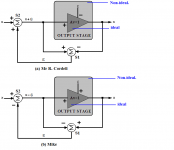
From this it is apparent that what's required is the provision of some means (S1) of subtracting the output of a non-ideal but nominally unity voltage-gain power output stage from its input, to isolate the error generated in said output stage {figure (b) below}.
Additionally, means (S2) must be provided to invert the extracted error ''e'', and algebraically sum the same with the input ''x'' to the power stage.
Clearly {figure (b)}, the gain modulus around the loop defined by summers S1 and S2 (with respect to the extracted error ''e'') must be exactly unity for complete error cancellation.
Mr Cordell's block-diagram interpretation {figure (a)} is algebraically correct, but i was of the view that, in the interest of intuitive and trouble-free implementation, the block diagram should have a close relationship with the synthesized circuitry, and conversely.
Note that Mr Cordell's circuit uses a common emitter transistor (Q22 and Q23) for S2, which necessarily inverts ''e'' as required to drive the output stage.
Comparing the modified block diagram {figure (b)} with Mr Cordell's synthesized system, it is more readily apparent that Q22 is a differential amplifier, with the input to the MOSFET power stage as its electrical point of reference. This is also true of its nominal complement Q23.
Using the modified block diagram {figure (b)}, it became more readily apparent that while Hawksford/Cordell use differentially driven single BJTs to simultaneously extract output stage error and invert said error (i.e. summers S1 and S2 are implemented by a single transistor), Yokoyama's figure 2 uses two stages: a much simpler, heavily degenerated and, consequently, far more linear emitter coupled pair for S1, and the current mirror/second-stage collector combination for S2.
Viz. in Yokoyama's implementation, the current mirror (fig. 2) provides the required invasion of the extracted error signal ''e'' shown in figure (b).
It was my view initially that the division of circuit functions in Yokoyama's arrangement affords superior linearity, accuracy and precision with respect to Hawksford/Cordell. This, however, was found to be not entirely correct. This is because (with both Hawksford/Cordell and Yokoyama) in order to obtain unity-gain transmission around the loop defined by summers S1 and S2, the load between the later and the input to the power stage must be resistively specified.
This is effected in Hawksford/Cordell by collector resistors R34/R35, and in Yokoyama by collector resistors ''21'' and ''22''.
While Hawksford/Cordell provide low impedance drive to properly define their collector loads, Yokoyama, for some unfathomable reason, felt compelled to merely reduce the load at his second stage output to the desired level by means of feedfoward resistors ''21'' and ''22''.
This, as previously noted, is bound to significantly increase distortion in the second stage as well as the output stage, since the later is bypassed (otherwise excluded) in some measure by the feedfoward path provided by ''21'' and ''22''. The position of the second stage in this respect is further compromised by the fact that Yokoyama eschews minor loop compensation for the relatively inferior shunt variety.
I was thus satisfied that the preceding observations probably explain why Yokoyama's THD+N results are significantly inferior to those of Mr Cordell's system.
Be that as it may, i am of the view that given its aforementioned advantages, Yokoyama's arrangement merits closer scrutiny.
The problems introduced by Yokoyama resistively loading his second stage may be eliminated by introducing a class-A emitter-follower between the second stage and the output stage.
The emitter-follower, biased by Yokoyama's current mirror {S2 in figure (b)}, then drives the power stage's input impedance shunted by the load-defining resistors ''21'' and ''22''.
As previously noted, further improvements can be made by, for instance, using independent voltage rails of greater modulus than those of the output stage; this would accommodate the compliance of an active current sink in place of the capacitively bootstrapped resistive tail for the error extractor.
PB2, i hope the quote below, taken from Mr Cordell's paper, and my preceding explanation have amply demonstrated the error of your observations.
janneman said:Mike,
Don't muddle the discussion with reality 😉!
Jan
Hi Jan
, and, not least, Ultima Thule and PB2,My modest understanding of this vexed but fascinating issue stems from Mr Cordell's peerless prose. Viz.
Here the output stage, being a source follower, is modeled as having exactly unity gain with an error voltage e(x) added.
This error represents any departure from unity gain, whether it is a linear departure due to less than unity gain, a distortion due to transconductance non-linearity or injected errors like power supply ripple.
A differential amplifier, represented by summer S1, merely subtracts the output from the input of the power stage to arrive at e(x).
This error signal is then added to the input of the power stage by summer S2 to provide that distorted input which is required for an undistorted output.
The idea above is also substantially expressed in Henri T. Pichal's patent abstract.
From this it is apparent that what's required is the provision of some means (S1) of subtracting the output of a non-ideal but nominally unity voltage-gain power output stage from its input, to isolate the error generated in said output stage {figure (b) below}.
Additionally, means (S2) must be provided to invert the extracted error ''e'', and algebraically sum the same with the input ''x'' to the power stage.
Clearly {figure (b)}, the gain modulus around the loop defined by summers S1 and S2 (with respect to the extracted error ''e'') must be exactly unity for complete error cancellation.
Mr Cordell's block-diagram interpretation {figure (a)} is algebraically correct, but i was of the view that, in the interest of intuitive and trouble-free implementation, the block diagram should have a close relationship with the synthesized circuitry, and conversely.
Note that Mr Cordell's circuit uses a common emitter transistor (Q22 and Q23) for S2, which necessarily inverts ''e'' as required to drive the output stage.
Comparing the modified block diagram {figure (b)} with Mr Cordell's synthesized system, it is more readily apparent that Q22 is a differential amplifier, with the input to the MOSFET power stage as its electrical point of reference. This is also true of its nominal complement Q23.
Using the modified block diagram {figure (b)}, it became more readily apparent that while Hawksford/Cordell use differentially driven single BJTs to simultaneously extract output stage error and invert said error (i.e. summers S1 and S2 are implemented by a single transistor), Yokoyama's figure 2 uses two stages: a much simpler, heavily degenerated and, consequently, far more linear emitter coupled pair for S1, and the current mirror/second-stage collector combination for S2.
Viz. in Yokoyama's implementation, the current mirror (fig. 2) provides the required invasion of the extracted error signal ''e'' shown in figure (b).
It was my view initially that the division of circuit functions in Yokoyama's arrangement affords superior linearity, accuracy and precision with respect to Hawksford/Cordell. This, however, was found to be not entirely correct. This is because (with both Hawksford/Cordell and Yokoyama) in order to obtain unity-gain transmission around the loop defined by summers S1 and S2, the load between the later and the input to the power stage must be resistively specified.
This is effected in Hawksford/Cordell by collector resistors R34/R35, and in Yokoyama by collector resistors ''21'' and ''22''.
While Hawksford/Cordell provide low impedance drive to properly define their collector loads, Yokoyama, for some unfathomable reason, felt compelled to merely reduce the load at his second stage output to the desired level by means of feedfoward resistors ''21'' and ''22''.
This, as previously noted, is bound to significantly increase distortion in the second stage as well as the output stage, since the later is bypassed (otherwise excluded) in some measure by the feedfoward path provided by ''21'' and ''22''. The position of the second stage in this respect is further compromised by the fact that Yokoyama eschews minor loop compensation for the relatively inferior shunt variety.
I was thus satisfied that the preceding observations probably explain why Yokoyama's THD+N results are significantly inferior to those of Mr Cordell's system.
Be that as it may, i am of the view that given its aforementioned advantages, Yokoyama's arrangement merits closer scrutiny.
The problems introduced by Yokoyama resistively loading his second stage may be eliminated by introducing a class-A emitter-follower between the second stage and the output stage.
The emitter-follower, biased by Yokoyama's current mirror {S2 in figure (b)}, then drives the power stage's input impedance shunted by the load-defining resistors ''21'' and ''22''.
As previously noted, further improvements can be made by, for instance, using independent voltage rails of greater modulus than those of the output stage; this would accommodate the compliance of an active current sink in place of the capacitively bootstrapped resistive tail for the error extractor.
PB2 said:The output stage is approximately unity gain, shown in your diagram as exactly unity and non-inverting, thus there must be positive feedback since if one path to the subtractor is negative feedback the other path must be positive. The gain is slightly less than one in real life and therefore there would be more gain in the positive path.
PB2, i hope the quote below, taken from Mr Cordell's paper, and my preceding explanation have amply demonstrated the error of your observations.
Here the output stage, being a source follower, is modeled as having exactly unity gain with an error voltage e(x) added.
Attachments

anatech said:Hi Mike,
Deletions as requested.
-Chris
Hi Mike,
Offset voltage 7.6V together with bias 740mA seems not quite optimal? 😉
Regards
Heinz!
Re: Consolidation of ideas.
No, Mikeks you've not amply demonstrated anything. I call them as I see them and you've thrown up a smoke screen here, and spun my words deliberately taking the incorrect interpretation of them. This is why I will really drop this particular point after this post. Let me remind you that you asked the question about positive feedback, suggesting something contrary to Cordell's and many other's view. If you don't like my answer perhaps others will offer an answer that is acceptable to you.
Now, let me point out a few things here. You speak of models and synthesized circuits, which you might simulate, in which case it is possible to have, or specify exact gains. This is not possible in real hardware, nothing is exact, there are tolerances involved. In good design we try to simulate at the extremes of gain and frequency for example, yes I've done it. The points I make sometimes refer to real hardware and other times models or synthesized circuits, you'll have to figure that out through context.
When you compare my statement about real hardware:
"The output stage is approximately unity gain"
to Bob Cordell's - obviously about models:
"is modeled as having exactly unity gain"
And claim that I'm in error, you've simply misinterpreted my statements. Pairing them up correctly we have this:
my statement about the model:
"shown in your diagram as exactly unity (gain)"
Bob Cordell's:
"is modeled as having exactly unity gain"
We are saying the same thing.
It is clear to me that there is a _path_ for positive feedback in the model. Yes, the positive feedback _signal_ nulls in the ideal case, but may, or may not null in real hardware due to tolerances. I'm not claiming that this is a serious issue, just that the path is there.
I don't enjoy conversations where my words are spun to suit one's needs. Indeed, your question was about positive feedback, your long rambling is about synthesized circuits - a smoke screen.
I'm done with this one, and I'll think twice about answering your questions in the future.
Happy Thanksgiving to all who celebrate!
Pete B.
mikeks said:
Hi Jan
My modest understanding of this vexed but fascinating issue stems from Mr Cordell's peerless prose. Viz.
The idea above is also substantially expressed in Henri T. Pichal's patent abstract.
From this it is apparent that what's required is the provision of some means (S1) of subtracting the output of a non-ideal but nominally unity voltage-gain power output stage from its input, to isolate the error generated in said output stage {figure (b) below}.
Additionally, means (S2) must be provided to invert the extracted error ''e'', and algebraically sum the same with the input ''x'' to the power stage.
Clearly {figure (b)}, the gain modulus around the loop defined by summers S1 and S2 (with respect to the extracted error ''e'') must be exactly unity for complete error cancellation.
Mr Cordell's block-diagram interpretation {figure (a)} is algebraically correct, but i was of the view that, in the interest of intuitive and trouble-free implementation, the block diagram should have a close relationship with the synthesized circuitry, and conversely.
Note that Mr Cordell's circuit uses a common emitter transistor (Q22 and Q23) for S2, which necessarily inverts ''e'' as required to drive the output stage.
Comparing the modified block diagram {figure (b)} with Mr Cordell's synthesized system, it is more readily apparent that Q22 is a differential amplifier, with the input to the MOSFET power stage as its electrical point of reference. This is also true of its nominal complement Q23.
Using the modified block diagram {figure (b)}, it became more readily apparent that while Hawksford/Cordell use differentially driven single BJTs to simultaneously extract output stage error and invert said error (i.e. summers S1 and S2 are implemented by a single transistor), Yokoyama's figure 2 uses two stages: a much simpler, heavily degenerated and, consequently, far more linear emitter coupled pair for S1, and the current mirror/second-stage collector combination for S2.
Viz. in Yokoyama's implementation, the current mirror (fig. 2) provides the required invasion of the extracted error signal ''e'' shown in figure (b).
It was my view initially that the division of circuit functions in Yokoyama's arrangement affords superior linearity, accuracy and precision with respect to Hawksford/Cordell. This, however, was found to be not entirely correct. This is because (with both Hawksford/Cordell and Yokoyama) in order to obtain unity-gain transmission around the loop defined by summers S1 and S2, the load between the later and the input to the power stage must be resistively specified.
This is effected in Hawksford/Cordell by collector resistors R34/R35, and in Yokoyama by collector resistors ''21'' and ''22''.
While Hawksford/Cordell provide low impedance drive to properly define their collector loads, Yokoyama, for some unfathomable reason, felt compelled to merely reduce the load at his second stage output to the desired level by means of feedfoward resistors ''21'' and ''22''.
This, as previously noted, is bound to significantly increase distortion in the second stage as well as the output stage, since the later is bypassed (otherwise excluded) in some measure by the feedfoward path provided by ''21'' and ''22''. The position of the second stage in this respect is further compromised by the fact that Yokoyama eschews minor loop compensation for the relatively inferior shunt variety.
I was thus satisfied that the preceding observations probably explain why Yokoyama's THD+N results are significantly inferior to those of Mr Cordell's system.
Be that as it may, i am of the view that given its aforementioned advantages, Yokoyama's arrangement merits closer scrutiny.
The problems introduced by Yokoyama resistively loading his second stage may be eliminated by introducing a class-A emitter-follower between the second stage and the output stage.
The emitter-follower, biased by Yokoyama's current mirror {S2 in figure (b)}, then drives the power stage's input impedance shunted by the load-defining resistors ''21'' and ''22''.
As previously noted, further improvements can be made by, for instance, using independent voltage rails of greater modulus than those of the output stage; this would accommodate the compliance of an active current sink in place of the capacitively bootstrapped resistive tail for the error extractor.
PB2, i hope the quote below, taken from Mr Cordell's paper, and my preceding explanation have amply demonstrated the error of your observations.
anatech said:Hi Mike,
Deletions as requested.
-Chris
Thanks Chris.
powerbecker said:
Hi Mike,
Offset voltage 7.6V together with bias 740mA seems not quite optimal? 😉
Regards
Heinz!
Yes.
Offset is unlikely to be optimal, open-loop, with a non-complementary class-A follower.
Reduce the bias voltage to 3.5V.,run the sim.,and select''view'',and then''spice error log'' to see THD.
Further suggestions and critical analysis are welcome. 🙂
Re: Re: Consolidation of ideas.
I am sorry if i appear to have misunderstood your post, Pete. This was not my intention.
However, with due respect, your response above is nonsensical from start to finish.
From my perspective, this is a very strange description of the workings of a differential amplifier:
Perhaps it's just as well you have decided not to demonstrate the presence of this vexatious positive feedback path, or, indeed, participate further.
Happy thanksgiving, Pete. 🙂
P.S. I have endeavoured to make things as obvious as possible below:
PB2 said:No, Mikeks you've not amply demonstrated anything. I call them as I see them and you've thrown up a smoke screen here, and spun my words deliberately taking the incorrect interpretation of them. This is why I will really drop this particular point after this post. Let me remind you that you asked the question about positive feedback, suggesting something contrary to Cordell's and many other's view. If you don't like my answer perhaps others will offer an answer that is acceptable to you.
Now, let me point out a few things here. You speak of models and synthesized circuits, which you might simulate, in which case it is possible to have, or specify exact gains. This is not possible in real hardware, nothing is exact, there are tolerances involved. In good design we try to simulate at the extremes of gain and frequency for example, yes I've done it. The points I make sometimes refer to real hardware and other times models or synthesized circuits, you'll have to figure that out through context.
When you compare my statement about real hardware:
"The output stage is approximately unity gain"
to Bob Cordell's - obviously about models:
"is modeled as having exactly unity gain"
And claim that I'm in error, you've simply misinterpreted my statements. Pairing them up correctly we have this:
my statement about the model:
"shown in your diagram as exactly unity (gain)"
Bob Cordell's:
"is modeled as having exactly unity gain"
We are saying the same thing.
It is clear to me that there is a _path_ for positive feedback in the model. Yes, the positive feedback _signal_ nulls in the ideal case, but may, or may not null in real hardware due to tolerances. I'm not claiming that this is a serious issue, just that the path is there.
I don't enjoy conversations where my words are spun to suit one's needs. Indeed, your question was about positive feedback, your long rambling is about synthesized circuits - a smoke screen.
I'm done with this one, and I'll think twice about answering your questions in the future.
I am sorry if i appear to have misunderstood your post, Pete. This was not my intention.
However, with due respect, your response above is nonsensical from start to finish.
From my perspective, this is a very strange description of the workings of a differential amplifier:
PB2 said:
....... if one path to the subtractor is negative feedback the other path must be positive......
Pete B.
Perhaps it's just as well you have decided not to demonstrate the presence of this vexatious positive feedback path, or, indeed, participate further.
Happy thanksgiving, Pete. 🙂
P.S. I have endeavoured to make things as obvious as possible below:
Attachments
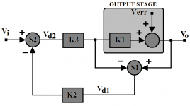
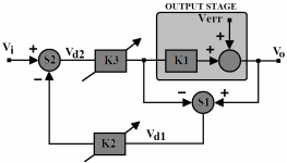
Let me try to clarify what I think Pete was saying, Mike. I've attached below a scan of some handwritten equations. This block diagram was intended to correspond to the semi-idealized error correction circuit I posted previously here. In this diagram, K1 represents the small-signal gain of the MOSFET follower, K2 is the resistor divider ratio, and K3 is the gain adjustment of the diff amp collector resistor. In general you want K1=K2. So I'd like to ask you three questions. Lets assume the linear case with Verr = 0.
1) How much feedback is there when K1=K2?
2) When K1 > K2, is the feedback positive or negative?
3) When K1 < K2, is the feedback positive or negative?
(Note: I had to click the magnify in Firefox to get decent legibility)
1) How much feedback is there when K1=K2?
2) When K1 > K2, is the feedback positive or negative?
3) When K1 < K2, is the feedback positive or negative?
(Note: I had to click the magnify in Firefox to get decent legibility)
Attachments
Positive feedback
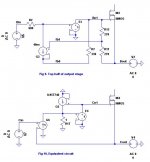
More analysis of the simplified model of Bob's output stage.
Fig 9. is the same as my previous fig 8 but is for the top half only. The behaviour is identical and the loop gain from output to FET gate is -23. This means that there is a negative feedback factor of 23 or about 27dB.
Bob's circuit is a little complicated because it contains an extra path in addition to that of Hawkford's model - made with R12. I believe this is there because it is an integral part of the bias circuit for the FETs. Bob has combined the bias circuit with the correction circuit. This adds another negative feedback path which must be taken into account. Note that fb0 is the positive feedback path and fb1 is the negative feedback path. fb1 is driven by both Bn1 and Bout (two NFB paths).
Fig 10. is an equivalent circuit. It performs identically. Here I have simplified the circuit by aggregating the feedback paths. I have created a current based summer with R1, fed by the input/output error signal from G6 and the positive feedback signal from G5. E4 is a unity gain buffer as before. The combination of E4 and G5 creates a gain block of value 1/(1 - a), as you may recall from fig 4 before, where a = 0.958. This gives the forward gain of 23 as before.
You may have noticed that the loop gain of 27dB is not the "infinity" that Hawksford's model requires for perfect correction (which is impractical). I would like to see what the loop gain is of the full Spice model plotted against frequency to confirm this finding.
Attachments
Thanks Andy, your model does illustrate the point I made,
Let me also offer this, derived from your model:
Vo = [K1*Vi + Verr(1 - K2*K3)]/(1 - K2*K3 + K1*K3)
Let me also offer this, derived from your model:
Vo = [K1*Vi + Verr(1 - K2*K3)]/(1 - K2*K3 + K1*K3)
andy_c said:Let me try to clarify what I think Pete was saying, Mike. I've attached below a scan of some handwritten equations. This block diagram was intended to correspond to the semi-idealized error correction circuit I posted previously here. In this diagram, K1 represents the small-signal gain of the MOSFET follower, K2 is the resistor divider ratio, and K3 is the gain adjustment of the diff amp collector resistor. In general you want K1=K2. So I'd like to ask you three questions. Lets assume the linear case with Verr = 0.
1) How much feedback is there when K1=K2?
2) When K1 > K2, is the feedback positive or negative?
3) When K1 < K2, is the feedback positive or negative?
(Note: I had to click the magnify in Firefox to get decent legibility)
andy_c said:Let me try to clarify what I think Pete was saying....
Hi Andy, 🙂
In view of the following, I don't think it's necessary to clarify Pete in any respect; your contribution is sufficient.

PB2 said:I'll pass on further discussion......Pete B.
PB2 said:I'm done with this one.....Pete B.
To continue, Andy, if non-ideal circuit characteristics are to be accommodated, then a second-level block diagram, such as yours, should demonstrate that the gain-modulus around the loop defined by the summers (with respect to the extracted error) may not be exactly unity (the condition required for complete error cancellation).
Note that, contrary to Lipshitz/Vanderkooy (''Is Zero Distortion
Possible With Feedback?'', AES Preprint #2170, Oct.1984: fig. 1d), i
am of the view that this is active negative feedback, and, moreover, constitutes error cancellation in fact.
Thus, to use your nomenclature, non-ideality in the gain provided by
the two summers, S1 and S2, may be represented by two gain blocks K2 and K3 respectively.
It is at this point, i am afraid, that i part company with your block-level interpretation of the system.
This is because your K2 and K3 represent gain/non-ideality in summer S1 while S2 remains ideal; i fail to see why, for instance, S1 has gain/non-ideality expressed at one input and not the other.
In fact, with a non-ideal summer (differential amplifiers included),
all conceivable gain/non-ideality, including mismatched input impedances, may be logically expressed at the ideal summer's output.
Thus:
Attachments
Error correction vs. negative feedback
In view of the ongoing debate regarding whether error correction is negative feedback in disguise or a different kind of animal altoghether, I prepared a condensed comparison trying to abstract implementation details.
Since combining text, graphics and math in a minimally readable form is not possible within a typical post, I choose to attach a PDF.
Please keep in mind notation - which departs with the one used here - harks back to almost 2 years, the time I originally started to work this issue.
Rodolfo
Attachments
mikeks said:i fail to see why, for instance, S1 has gain/non-ideality expressed at one input and not the other.
Okay, this gets to the core of what I was trying to convey, and the relationship of my block diagram (with the K1, K2 and K3) to the semi-idealized SPICE sim I posted here. The following text refers to elements in the schematic of that sim, so you'll need to open up that schematic to see what I'm saying here.
You've mentioned previously that the Hawksford error correction is somewhat voltage-inefficient. Certainly it makes sense to make the best possible use of the available voltage swing at the diff amp output. How do we do this? Consider the idealized diff amp with K2 and K3 equal to one. I claim that in my sim, that corresponds exactly to R12=Rsh=infinity, and C1=0. In that case R5 and R6 just average the DC voltages at the MOSFET gates to near zero. Now with the diff amp collector resistor chosen correctly in terms of its gm to get a gain of exactly 1, this gives K3=1. Now we set Rsh=infinity, delete C1, and do a transient sim with a nice large sine wave output signal. We observe the voltage across the diff amp collector resistors R1 and R2. What does it look like? Well, it looks like an almost perfect sine wave at the fundamental. Why? Because the error correction is trying to set the gain to exactly 1, while the actual small-signal gain of the MOSFETs is really something like 0.95 or so. In my block diagram, this MOSFET small-signal gain is represented by K1.
So as the output signal becomes large, the dynamic range of the error correction is being wasted by an essentially useless linear gain correction. We can fix this. Let's first assume for the sake of argument that the MOSFET bandwidth is infinite. By choosing Rsh appropriately so the voltage divider "gain" K2 is deliberately set to the "gain" of the MOSFET follower, then the difference mode input voltage to the diff amp will be zero, except for the distortion. This wasn't true before because of the gain discrepancy. Let's first assume we make no correction of the diff amp collector resistor. If we do our transient sim now, we find that the error correction voltage across the resistors consists almost entirely of distortion, and is way smaller in amplitude than it was before. We have therefore gained the following: We have either increased how much distortion we can compensate for with a given DC drop across the diff amp collector resistors, or we can compensate for the same distortion with a smaller drop. But you'll find after doing this that we can no longer obtain a perfect distortion null. To fix this, the diff amp collector resistors must be adjusted. That's where K3 comes in. If we adjust K3 so that K2*K3=1 as my analysis shows, we get our perrfect null back. That's equivalent to adjusting the diff amp collector resistors. Indeed, in the .PARAM statements of the sim you can see that as the voltage divider ratio is varied, the collector resistors adjust automatically to get the equivalent of K2*K3=1 in my block diagram. This assumes that changes to the divider are done using the .PARAM statements and not editing the part value directly. None of this is an accident. It came about as I was trying to fix the dynamic range problem. After doing so, I lost my distortion null. The block diagram of my previous post was a direct result of that problem and my head-scratching to find a solution.
So to make a long story short, K2 is there to maximize the available dynamic range of the error correction, while K3 is there to "fix up" the distortion null that we lost by making K2 not equal to one. But these could also be used to model another useful, practical situation. Namely, K2 could be a voltage divider with a pot. We could trim it to get a distortion null, provided the diff amp collector resistors were appropriately chosen.
By the way, think of K3 as two blocks in cascade: a transconductance gm and collector resistor RC. Then the input summer is just the KVL equation assuming an ideal voltage source input.
mikeks said:ingrast, what is the rationale for the term (1/A')?
It has been customary to assume plant gain as unity (eg emitter follower etc.) but in fact the concept is valid for arbitrary gain plants.
Conceptually what we seek is to compare the plant input with a correspondingly scaled output, and here is where 1/A' enters.
If you check the gain expression and for a moment asume 1/S -B =0, then system gain is given *exactly* by A'.
Rodolfo
PS. It makes sense to make A'=Ao where Ao is for example the nominal plant gain, but this condition is not necessary for the system to work, it self adjusts to set total gain to A'.
andy_c said:Okay, this gets to the core of what I was trying to convey, and the relationship of my block diagram (with the K1, K2 and K3) to the semi-idealized SPICE sim I posted here. The following text refers to elements in the schematic of that sim, so you'll need to open up that schematic to see what I'm saying here.
Hi Andy,
Thanks for that.
I would be extremely careful when using block diagrams to represent a system.
Elements used for convenience in a SPICE model, for instance, and which may not be of relevance in the real system, really shouldn't put in an appearance in a second level block diagram.
andy_c said:
So to make a long story short, K2 is there to maximize the available dynamic range of the error correction, while K3 is there to "fix up" the distortion null that we lost by making K2 not equal to one.
See below:
Attachments
mikeks said:Elements used for convenience in a SPICE model, for instance, and which may not be of relevance in the real system, really shouldn't put in an appearance in a second level block diagram.
Ah, but it is of real relevance in a practical system. Have a look at the pot in the Halcro circuit. It implements unequal scale factors ahead of your summer S1. Notice also that this adjustable scale factor is picked off from the input of the MOSFET stage, just like my diagram. Further, the output of K3 in my block diagram corresponds exactly to the product of IC*RC in the error correction diff amp. Likewise, the output of the summer at the system input in my diagram corresponds exactly to the collector voltage of the error correction diff amp output. This works for both my sim and the Halcro.
The block diagram you just posted has no such relationship, nor does it fix the dynamic range problem when there's only one or a small numbe of FETs in parallel.
- Home
- Amplifiers
- Solid State
- Bob Cordell Interview: Error Correction