Re: Re: hec != hoax ?
Thank you Bob.
That's right, I came up with this afterwards.
OK, your amp does not run out of steam, it was our amp that shows this potential problem as lateral MOSFET were used, having a much lower trans-conductance and gate threshold voltage.
I'm afraid you are confusing me with someone else. As far as I know I don't even have a model of the IRFP244.
That's right, the Toshibas need less gate drive voltage. At high drain currents, Vgs is of the same order as the drain-source saturation voltage, so almost nothing is gained by driving Vgs beyond the supply voltage. Besides, I don't like this practice at all, as Cgd is skyrocketing under such conditions and is a potential source of instabilities and cross-conductance.
Regarding boosted supplies, my NAD-319 has them too, comprising of 6 diodes, 4 trannies, 2 zeners, 12 electrolytics, 4 caps and 16 resistors, that is, 44 additional components to squeeze a few more volts out of the OPS. Indeed, no big deal.
Cheers, Edmond.
Bob Cordell said:Hi Edmond,
Nice work. I always like it when someone shows that there is more than one way to skin a cat.
Thank you Bob.
Why didn't you use this circuit in your PGP instead of EC? 🙂. I assume you came up with this afterwards.
That's right, I came up with this afterwards.
I do have to take issue with a couple of things you said about EC.
The EC circuit does not run out of steam under heavy loads. Just look at my Figure 20 in my MOSFET amplifier paper, where I drove over 22 Amps into a 1 ohm load at 20 kHz with a 2-cycle burst, using only a single pair of output devices.
OK, your amp does not run out of steam, it was our amp that shows this potential problem as lateral MOSFET were used, having a much lower trans-conductance and gate threshold voltage.
I do recall that you showed a simulation of that where the error difference transistors were clipping, but in that simulation you were taking liberties with the design and using faulty MOSFET models. You added 0.22 ohm source resistors without accounting for their 4V drop at 20 amps. You also used an IRFP244 with a wimpy model that only put out 8.8 amps with a forward gate voltage of 7V. The IRFP240 data sheet shows 21 Amps at 7V.
I'm afraid you are confusing me with someone else. As far as I know I don't even have a model of the IRFP244.
The original EC circuit was designed to put out between 8 and 9V of turn-on voltage with respect to the output rail. As long as that capability is properly matched with the output devices, the EC circuit will not run out of steam.
In your circuit you are also taking advantage of the lower turn-on voltage of the Toshiba MOSFETs.
In more recent designs I use folded emitter followers to drive the EC, with the voltage spreading taking place after the folded EF, so the bias voltage is not stolen from the VAS. Moreover, no matter what you do, you need to have enough drive voltage ultimately to adequately forward bias the output MOSFETs. If you choose not to use a boosted supply anywhere, you are certainly free to do so, but you may be putting an unnecessarily large main high current power supply voltage on the output devices, dissipating more than need be. If one wishes to make such a compromise, it can be done with EC as well.
Nevertheless, your interesting design is about efficeint as one can get as long as you don't want to be able to swing the gate beyond the supply voltage. The use of the Toshibas makes this less of an issue anyway.
That's right, the Toshibas need less gate drive voltage. At high drain currents, Vgs is of the same order as the drain-source saturation voltage, so almost nothing is gained by driving Vgs beyond the supply voltage. Besides, I don't like this practice at all, as Cgd is skyrocketing under such conditions and is a potential source of instabilities and cross-conductance.
I generally like boosted supplies, and if you use one, a difference of a couple of volts one way or the other is no big deal. The boosted supplies are relatively inexpensive due to the low current needs, and the bit of extra headroom they give the VAS can help performance. Just a matter of choice. But in a truly high-performance amplifier a boosted supply is no big deal.
Cheers,
Bob
Regarding boosted supplies, my NAD-319 has them too, comprising of 6 diodes, 4 trannies, 2 zeners, 12 electrolytics, 4 caps and 16 resistors, that is, 44 additional components to squeeze a few more volts out of the OPS. Indeed, no big deal.
Cheers, Edmond.
traderbam said:Edmond,
This isn't a new topology but it is an effective alternative way to apply NFB to the FETs using 8 transistors. There are pros and cons. I agree with your hypothesis that similar performance is caused by similar NFB; implying HEC is not doing any error cancelling or other hocus pocus.
Brian
Hi Brian,
At least one point we agree on. 🙂
OK, it's not new. I doesn't matter as my primary goal was to show the equivalence between HEC and NFB. Nevertheless I like to see similar topologies. Do you have a schematic or just a link?
Cheers, Edmond.
hec != hoax ?
Hi Glen,
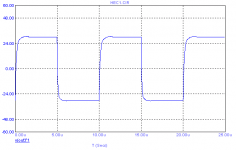
I don't think you have to worry about the stability, as the overshoot I was talking about has nothing to with violation of Bode's rules for stability. It was obviously caused by another mechanism. How else would you explain that the overshoot has gone in my 3rd version with the Schottky diodes?
BTW, have a look at the square wave response of HEC and compare that one with the figure in post 2695. 😀
Cheers, Edmond.
G.Kleinschmidt said:😎
That miller comp mod will give you a better PSRR too. But don't be too complacent about a little bit of overshoot in the OPS.
It may be masked by the closed loop gain in a complete amp, but the open loop gain is effected and the amplifier can have a reduced gain margin at the frequency peak, causing conditional stability issues (especially bursts of oscillation of the leading edges when going in and out of clipping.
Cheers,
Glen
Hi Glen,
I don't think you have to worry about the stability, as the overshoot I was talking about has nothing to with violation of Bode's rules for stability. It was obviously caused by another mechanism. How else would you explain that the overshoot has gone in my 3rd version with the Schottky diodes?
BTW, have a look at the square wave response of HEC and compare that one with the figure in post 2695. 😀
Cheers, Edmond.
Attachments
Re: Re: Re: hec != hoax ?
Hi Edmond,
I'm sorry if I confused you with someone else who did the simulation I was referring to.
I agree that the ability to drive the gates to the supply or beyond is in some cases questionable and somewhat output device dependent. But, as I pointed out, that is not the only benefit of using boosted supplies for the VAS and drivers.
The NAD example is surely a red herring. If someone chooses to add 44 extra components to achieve boosted supplies they are free to do it. It need not take more than one very small transformer, a pair of bridge rectifiers and some filter capacitors.
Cheers,
Bob
Edmond Stuart said:
I'm afraid you are confusing me with someone else. As far as I know I don't even have a model of the IRFP244.
That's right, the Toshibas need less gate drive voltage. At high drain currents, Vgs is of the same order as the drain-source saturation voltage, so almost nothing is gained by driving Vgs beyond the supply voltage. Besides, I don't like this practice at all, as Cgd is skyrocketing under such conditions and is a potential source of instabilities and cross-conductance.
Regarding boosted supplies, my NAD-319 has them too, comprising of 6 diodes, 4 trannies, 2 zeners, 12 electrolytics, 4 caps and 16 resistors, that is, 44 additional components to squeeze a few more volts out of the OPS. Indeed, no big deal.
Cheers, Edmond.
Hi Edmond,
I'm sorry if I confused you with someone else who did the simulation I was referring to.
I agree that the ability to drive the gates to the supply or beyond is in some cases questionable and somewhat output device dependent. But, as I pointed out, that is not the only benefit of using boosted supplies for the VAS and drivers.
The NAD example is surely a red herring. If someone chooses to add 44 extra components to achieve boosted supplies they are free to do it. It need not take more than one very small transformer, a pair of bridge rectifiers and some filter capacitors.
Cheers,
Bob
Re: Re: Re: Re: hec != hoax ?
Hi Bob,
If you feel happy with an unregulated PSU, okay, but, apparently, NAD had some reasons to choose for a regulated PSU. So let's call it a 'pink herring'.
Cheers, Edmond.
Bob Cordell said:Hi Edmond,
[snip]
The NAD example is surely a red herring. If someone chooses to add 44 extra components to achieve boosted supplies they are free to do it. It need not take more than one very small transformer, a pair of bridge rectifiers and some filter capacitors.
Cheers,
Bob
Hi Bob,
If you feel happy with an unregulated PSU, okay, but, apparently, NAD had some reasons to choose for a regulated PSU. So let's call it a 'pink herring'.
Cheers, Edmond.
Re: Re: Re: Re: Re: hec != hoax ?
Hi Edmond,
Fair enough. I do in fact like a regulated PSU for the input/VAS, but I just see that as a separate issue.
I'm curious, does NAD regulate the main high-current rails to the output stage?
Cheers,
Bob
Edmond Stuart said:
Hi Bob,
If you feel happy with an unregulated PSU, okay, but, apparently, NAD had some reasons to choose for a regulated PSU. So let's call it a 'pink herring'.
Cheers, Edmond.
Hi Edmond,
Fair enough. I do in fact like a regulated PSU for the input/VAS, but I just see that as a separate issue.
I'm curious, does NAD regulate the main high-current rails to the output stage?
Cheers,
Bob
Off topic
Hi Bob,
No, the main high-current rails are unregulated. BTW, I have spiced the NAD and it appears that the PSRR of the front end is rather low, about 60dB. Probably, that's the reason why the front end has a regulated PSU.
Cheers, Edmond.
Bob Cordell said:Hi Edmond,
Fair enough. I do in fact like a regulated PSU for the input/VAS, but I just see that as a separate issue.
I'm curious, does NAD regulate the main high-current rails to the output stage?
Cheers,
Bob
Hi Bob,
No, the main high-current rails are unregulated. BTW, I have spiced the NAD and it appears that the PSRR of the front end is rather low, about 60dB. Probably, that's the reason why the front end has a regulated PSU.
Cheers, Edmond.
Re: hec != hoax ?
OK, but I saw your Schottky diode version after. How do you explain it?
Cheers,
Glen
Edmond Stuart said:
Hi Glen,
I don't think you have to worry about the stability, as the overshoot I was talking about has nothing to with violation of Bode's rules for stability. It was obviously caused by another mechanism. How else would you explain that the overshoot has gone in my 3rd version with the Schottky diodes?
BTW, have a look at the square wave response of HEC and compare that one with the figure in post 2695. 😀
Cheers, Edmond.
OK, but I saw your Schottky diode version after. How do you explain it?
Cheers,
Glen
Re: Re: Re: hec != hoax
Seems there's current gain in Q2/Q3 with the voltage gain showing up at Q5/Q6.
Did you consider simply having Q5/Q6, and no mirror?
1 GV/s ... putting on your marketing hat now?
Reminds me of the old National video buffers.
Pete B.
Edmond Stuart said:
....
The VASes consists of Q5 and Q6 (not Q2 and Q3). As they are part of the current mirrors, the current gain is of course rather low, in fact unity.
....
BTW, the slew rate is 1GV/s 😀
Cheers, Edmond.
Seems there's current gain in Q2/Q3 with the voltage gain showing up at Q5/Q6.
Did you consider simply having Q5/Q6, and no mirror?
1 GV/s ... putting on your marketing hat now?
Reminds me of the old National video buffers.
Pete B.
Re: Re: hec != hoax ?
Hi Glen,
I can't explain it. Actually, I was fooled by the simulator. When I applied a square wave with non-zero rise and fall times, the overshoot (about 5%) was back. So, if that little overshoot is really a problem, one can use the compensation as shown in post #2694.
BTW, this time I have spiced a HEC OPS with the same trannies and the same Fc of the compensation and, surprisingly, the phase lag at 2MHz is 18 deg. opposed to 15 deg. of the NFB OPS. 😀
Cheers, Edmond.
G.Kleinschmidt said:OK, but I saw your Schottky diode version after. How do you explain it?
Cheers,
Glen
Hi Glen,
I can't explain it. Actually, I was fooled by the simulator. When I applied a square wave with non-zero rise and fall times, the overshoot (about 5%) was back.
So, if that little overshoot is really a problem, one can use the compensation as shown in post #2694.BTW, this time I have spiced a HEC OPS with the same trannies and the same Fc of the compensation and, surprisingly, the phase lag at 2MHz is 18 deg. opposed to 15 deg. of the NFB OPS. 😀
Cheers, Edmond.
Re: Re: Re: Re: hec != hoax
Hi Pete,
It depends on you point of view. The input signal 'sees' current gain in Q2/Q3, while the FB signal does not, as now these trannies operate in common base mode.
Certainly not, and for several reasons. With no mirror, the unity gain crossover frequency of the Miller gets too high and the phase margin too small. Also, it's more difficult to get a well defined and stable quiescent current of Q5/Q6.
Indeed, 1GV/s (or should I say 1000V/us?) seems ridiculous high, but that's what my simulator tolds me. OTOH, HEC slews at half that speed. So, it's probably wise to see these numbers in a more relative perspective.
Cheers, Edmond.
PB2 said:Seems there's current gain in Q2/Q3 with the voltage gain showing up at Q5/Q6.
Hi Pete,
It depends on you point of view. The input signal 'sees' current gain in Q2/Q3, while the FB signal does not, as now these trannies operate in common base mode.
Did you consider simply having Q5/Q6, and no mirror?
Certainly not, and for several reasons. With no mirror, the unity gain crossover frequency of the Miller gets too high and the phase margin too small. Also, it's more difficult to get a well defined and stable quiescent current of Q5/Q6.
1 GV/s ... putting on your marketing hat now?
Reminds me of the old National video buffers.
Pete B.
Indeed, 1GV/s (or should I say 1000V/us?) seems ridiculous high, but that's what my simulator tolds me. OTOH, HEC slews at half that speed. So, it's probably wise to see these numbers in a more relative perspective.
Cheers, Edmond.
Re: Re: Re: Re: Re: hec != hoax
Hi Edmond,
Although I was very pleased that my 25 year-old 50 Watt MOSFET amplifier had a slew rate of 300 V/us, I think that anything over 100 V/us is probably gravy as long as linearity is good in the whole design and that no circuit except the output transistors has to go out of Class A to get there.
Cheers,
Bob
Edmond Stuart said:
Hi Pete,
It depends on you point of view. The input signal 'sees' current gain in Q2/Q3, while the FB signal does not, as now these trannies operate in common base mode.
Certainly not, and for several reasons. With no mirror, the unity gain crossover frequency of the Miller gets too high and the phase margin too small. Also, it's more difficult to get a well defined and stable quiescent current of Q5/Q6.
Indeed, 1GV/s (or should I say 1000V/us?) seems ridiculous high, but that's what my simulator tolds me. OTOH, HEC slews at half that speed. So, it's probably wise to see these numbers in a more relative perspective.
Cheers, Edmond.
Hi Edmond,
Although I was very pleased that my 25 year-old 50 Watt MOSFET amplifier had a slew rate of 300 V/us, I think that anything over 100 V/us is probably gravy as long as linearity is good in the whole design and that no circuit except the output transistors has to go out of Class A to get there.
Cheers,
Bob
Re: Re: Re: Re: Re: Re: hec != hoax
Hi Bob,
I fully agree with that, but don't misunderstand me. I wasn't hunting for an extreme high slew rate. Just see it as an unintentional spin-off.
BTW, your 300V/us refers to a complete amp, while my 1GV/s refers only to the OPS. In a complete amp this figure will never be reached, as the VAS or IPS or both will slow it down.
Cheers, Edmond.
Bob Cordell said:Hi Edmond,
Although I was very pleased that my 25 year-old 50 Watt MOSFET amplifier had a slew rate of 300 V/us, I think that anything over 100 V/us is probably gravy as long as linearity is good in the whole design and that no circuit except the output transistors has to go out of Class A to get there.
Cheers,
Bob
Hi Bob,
I fully agree with that, but don't misunderstand me. I wasn't hunting for an extreme high slew rate. Just see it as an unintentional spin-off.
BTW, your 300V/us refers to a complete amp, while my 1GV/s refers only to the OPS. In a complete amp this figure will never be reached, as the VAS or IPS or both will slow it down.
Cheers, Edmond.
so, who's gonna be the first to really build bob's 25 year old design and use modern semiconductors?
😀
mlloyd1
😀
mlloyd1
models?
I might do a few quick sims of this circuit and I want to be sure to use the same models. Are these the final versions that you used for these sims? Just to confirm:
http://www.diyaudio.com/forums/showthread.php?postid=1318471#post1318471
http://www.diyaudio.com/forums/showthread.php?postid=1323417#post1323417
Pete B.
Edmond Stuart said:And here is a version without any overshoot and a phase lag of 15 deg. at 2MHz.
Cheers, Edmond.
I might do a few quick sims of this circuit and I want to be sure to use the same models. Are these the final versions that you used for these sims? Just to confirm:
http://www.diyaudio.com/forums/showthread.php?postid=1318471#post1318471
http://www.diyaudio.com/forums/showthread.php?postid=1323417#post1323417
Pete B.
Re: models?
Hi Pete,
That are the final versions, but up till now, I have used the BSIM3.3 models and Vto=+/-2.4V in stead. The next thing I'll do is also using the EKV models.
Cheers, Edmond.
PB2 said:I might do a few quick sims of this circuit and I want to be sure to use the same models. Are these the final versions that you used for these sims? Just to confirm:
http://www.diyaudio.com/forums/showthread.php?postid=1318471#post1318471
http://www.diyaudio.com/forums/showthread.php?postid=1323417#post1323417
Pete B.
Hi Pete,
That are the final versions, but up till now, I have used the BSIM3.3 models and Vto=+/-2.4V in stead. The next thing I'll do is also using the EKV models.
Cheers, Edmond.
traderbam said:Edmond,
This isn't a new topology but it is an effective alternative way to apply NFB to the FETs using 8 transistors. There are pros and cons. I agree with your hypothesis that similar performance is caused by similar NFB; implying HEC is not doing any error cancelling or other hocus pocus.
Brian
Hi Brian,
Where is the schematic that shows it's not new?
Furthermore, wouldn't it be nice if you elaborate on the pros and cons you are foreseeing?
Cheers, Edmond.
In my lab notebook, Edmond. Besides, this is a very common phase splitting arrangement so I imagine it has been invented many times. This doesn't mean you are any less a man, though.
Pros and cons? You still haven't answered my questions.
Pros and cons? You still haven't answered my questions.
traderbam said:In my lab notebook, Edmond. Besides, this is a very common phase splitting arrangement so I imagine it has been invented many times. This doesn't mean you are any less a man, though.
Pros and cons? You still haven't answered my questions.
Hi Brian,
So, in you lab notebook. May we have a look at it?
Phase splitter? There ain't no phase splitter, only two phase inverters (i.e. the current mirrors).
>You still haven't answered my questions.
Which question? Perhaps you mean how I've measured the 'sonic performance'. You know that nobody has the tools to measure that objectively.
Anyhow, if someone starts talking about pros and cons, the least he can do is telling us what kind of pros and cons, in stead of making a simplistic statement without any clue.
Cheers, Edmond.
Practical aspects of error correction
A couple of times people have expressed concern about the need to adjust the pot in the EC circuit (if you have chosen to implement it with a pot).
As amplifiers using EC are usually going to be delivering very low amounts of distortion, the question comes up of how to do such an adjustment without an expecially sensitive THD analyzer.
One approach that I have used is to tap off the signal that enters the error-correcting output stage of the amplifier in closed-loop operation. This is essentially the VAS signal, but wants to be the buffered version of it. A resistive center tap off of the first emitter follower pair in the EC circuit works well.
If you look at this node, it essentially contains the inverse of the output stage distortion, since the global feedback tends to drive the distortion at the output of the amplifier to zero. With this view of the essentially raw distortion of the output stage (which will typically be well above 0.001%), it is easy to tweak the pot for a minimum of the distortion at 1 kHz, since this is a static balance of the EC stage that you are shooting for.
Moreover, it is best to make this adjustment at a reduced power level where crossover distortion is relatively greatest. For a vertical MOSFET amp this might be in the vicinity of 9V peak into an 8-ohm load, but will be design dependent. Even better, do it into a 4 ohm load.
Due to slight nonlinearities in the simple versions of the EC circuit (like the one I used a long time ago), the optimum pot setting for EC performance is not necessarily the same at low power as at high power. It is better to optimize at low power where crossover distortion is the concern, because the big reduction in crossover distortion is one of the most important features of error correction.
Cheers,
Bob
- Home
- Amplifiers
- Solid State
- Bob Cordell Interview: Error Correction