I think there is a reasoning for non-global NFB design, or at least for output stage outside global NFB.
- rock solid stability, as the output stage does not bring non-linear phase shifts into global NFB
- disturbances are not fed back to an input of differential input stage
- no need neither for output coil, nor Zobel
- output impedance like 0.05 ohm is achievable
- distortion does not depend on frequency in audio band and doesn not increase with frequency
PMA said:I think there is a reasoning for non-global NFB design, or at least for output stage outside global NFB.
- rock solid stability, as the output stage does not bring non-linear phase shifts into global NFB
- disturbances are not fed back to an input of differential input stage
- no need neither for output coil, nor Zobel
- output impedance like 0.05 ohm is achievable
- distortion does not depend on frequency in audio band and doesn not increase with frequency
Hi Pavel,
"output impedance like 0.05 ohm is achievable"? Even without any kind of NFB? OK, maybe in case of a class-heat BJT output stage, but in all other cases I have my doubts if this is achievable.
Cheers, Edmond.
traderbam said:[snip]
I also believe that an expertly designed high feedback design should have no sound of its own, which is best of all.
[snip]


Local feedback (s) in output stage. My EC output stage with 350mA iddle current has this output impedance as well.
I have not said without any NFB. I have exactly said output stage outside global NFB. I mean output stage with voltage gain close to 1.
Edit: this one:
I have not said without any NFB. I have exactly said output stage outside global NFB. I mean output stage with voltage gain close to 1.
Edit: this one:
Attachments
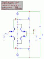
PMA said:Local feedback(s) in output stage. My EC output stage with 350mA iddle current has this output impedance as well.
I have not said without any NFB. I have exactly said output stage outside global NFB. I mean output stage with voltage gain close to 1.
Edit: this one:
Hi Pavel,
My apologies for overlooking the word: "global".
When time permits, I'll have a closer look at your intriguing circuit.
On the other hand, does it really matter whether a FB loop encompasses just one tranny or ten, or whether it is local or global, IF the FB loop is rock stable? IMHO, I don't think so.
Cheers, Edmond.
Hi Edmond,
Just make both and compare. These never ending debates only consume time of us all.
BTW, that last shown output stage is also inside global NFB. It was to show you low output impedance.
It is only the class A CFP output that I use outside global NFB. And it is the best amp I have ever made.
Regards,
Pavel
janneman said:Edmond,
I think I know why the red curve is just below 0dB instead of just above. IIRC Bob's ec circuit uses single transistors to extract the error. The error gain is less than one, while ideally it should be exactly one. if you would replace those transistors with an 'ideal' gain-of-one, the red curve should be just above one, in fact as much above one as the output stage gain is below one.
Jan Didden
Hi Jan,
I agree with you that something is wrong with the red curve, although it's far too high, not too low, but why? I really don't know at this moment. I've been poking with Middlebrook's well-proved gain probe at different places, but failed to get the correct answer.
OTOH, what's this "error gain"? Are we at cross purposes?
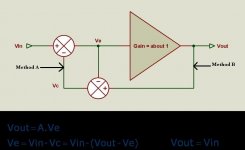
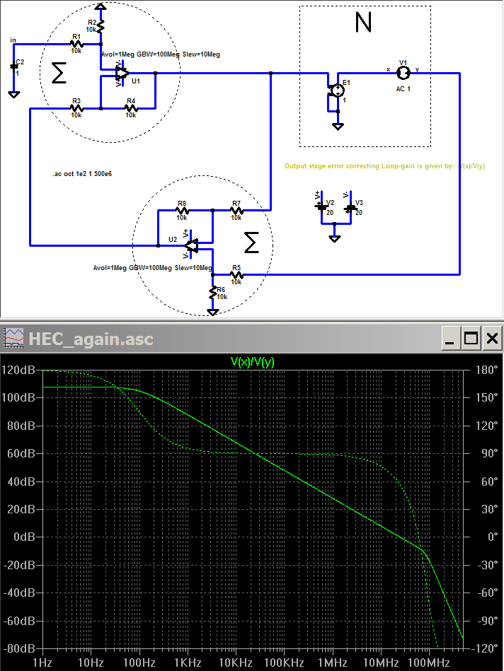
The red curve represents the loop gain at the input summer, see below, at point A.
This loop gain should normally below 1, in fact 1-N , where N is the gain of the output stage proper and b = 1.
According to my simulation the gain of the OPS = 0.93, so the "red" loop gain should 0.07 or -23dB and not -3.3dB or so.
Allow me some time to figure this out (also to clean up the schematics, so the numbering of components is in accordance with the original diagram of Bob).
Cheers, Edmond.
Attachments
Edmond Stuart said:
Hi Jan,
I agree with you that something is wrong with the red curve, although it's far too high, not too low, but why? I really don't know at this moment. I've been poking with Middlebrook's well-proved gain probe at different places, but failed to get the correct answer.
OTOH, what's this "error gain"? Are we at cross purposes?
The red curve represents the loop gain at the input summer, see below, at point A.
This loop gain should normally below 1, in fact 1-N , where N is the gain of the output stage proper and b = 1.
According to my simulation the gain of the OPS = 0.93, so the "red" loop gain should 0.07 or -23dB and not -3.3dB or so.
Allow me some time to figure this out (also to clean up the schematics, so the numbering of components is in accordance with the original diagram of Bob).
Cheers, Edmond.
Yes Edmond, I reached that conclusion as well. Something isn't kosher here. I remember an earlier sim of yours (?) that came out to -33dB, which was more in line with the expectations. And thanks for the effort, appreciate it.
Jan Didden
Brian, jcx, Edmond,
I have read your collective posts again and again in trying to distill the crux of our discussion to allow myself to be convinved 😱 . I've rewritten this several times to try to express myself clearly. At the risk of falling on my face, please take a look at this:
I think my argument on where to break the loop hinges on the legality of this: that I can replace the error summer, which takes it's inputs from both the input and the output of the N block, with another block, that takes it's input from N's output only but has a transfer function of [(1/N)-1]. If I would be allowed to do that, we only would have a single loop and then it doesn't matter anymore where you break the loop to measure its gain. Needless to say, in this case, the loop gain becomes 1-N.
Both Brian and jcx have said that this is not legal because the transfer function 1/N is not the conjugate to N, assuming that N is a complex function. I understand that, and that was something I had not realised before. But let me explore this a bit further.
Let us start at DC. Can I say, that at DC, 1/N is the conjugate to N. If that is true, at least at DC, the transformation I described above is legal and we have a single loop.
Again, at the risk of falling on my face, let me continue as if at DC this is indeed legal. The next question then would be, at what point, away from DC, does it start to become illegal? If, for the sake of argument, we assume that all the summing blocks etc have infinite bandwidth, we need only to concern ourselves with the N block.
It stands to reason that as we move away fom DC the argument doesn't immediately fall apart completely. I am running on intuition now, but would suggest that until we reach the corner frequency of N, the legality of the transformation substantially holds. It may start to deteriorate much earlier than that, or it may hold right up to that point. But there would be a region from DC upwards in frequency where my transformation would be allowed.
Please let me know what you think of this, and thanks for your patience.
Jan Didden

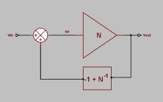
Ok, good. Your single block with N-1 is fine. You are absolutely right that this arrangement completely eliminates the output error. This is the block diagram that you really want to be able to build in a real circuit, right?
Now, do you consider the system to involve feedback from the output? I think you do. If so, how would you determine how much feedback there is?
Now, do you consider the system to involve feedback from the output? I think you do. If so, how would you determine how much feedback there is?
EC loop gain
Thanks Brian.
It appears that "our" gain and phase responses are almost identical.
Cheers, Edmond.
traderbam said:Good work Edmond. You might find posts 1325+ of interest.
Thanks Brian.
It appears that "our" gain and phase responses are almost identical.
Cheers, Edmond.
janneman said:Yes Edmond, I reached that conclusion as well. Something isn't kosher here. I remember an earlier sim of yours (?) that came out to -33dB, which was more in line with the expectations. And thanks for the effort, appreciate it.
Jan Didden
Hi Jan,
I've discovered what I did wrong. As you know, the EC stage is symmetrical. So, there are two sensing trannies (Q22 and Q23 in Bob's schematic) which transfer the error signal to the input summers (actually subtracters, but that's another story)
As both signals are equal in magnitude, I have fallen into a trap by assuming that just one gain probe inserted into one of two signal paths was sufficient. No! Completely wrong!
As I'm lazy, in particular regarding math, I did not use a second gain probe and adjust the all the equations. In stead, I combined the signal paths to a single one by using huge caps and inductors.
Now the red curves look OK.
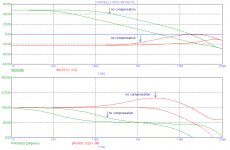
Also, I increased R34 and R35 to 730 Ohm to show the effect on the "green" loop gain (+50dB @ AF)
Although, my previous 'red' graphs were wrong, my final conclusions are still the same, because the correct loop transfer function at the input summer still doesn't unambiguously predict instability troubles.
Please, have a look at the uncompensated phase response at 18MHz: a seemingly sound phase margin of 180 degrees, yet the system is unstable.
Cheers, Edmond.
Attachments
Updated a realisticly limited implementaiton of the EC summers
I showed some time ago in this thread that the loop gain can be calculated as 1/2 * (a1 * a2) / (2 + a1 + a2)
The V1 source measures the loop gain around the output stage, the inverse gain plot would be the amount a (additive) error in the N gain block is attenuated == the amount of "Error Correction"
Trimming of the loop gain is simulated below by B1 behaviorial source simulating a time dependent resistance controlling the gain of the U2 sum, B1 ramps at 100 Ohms/100 uS giving 10K at 10 ms
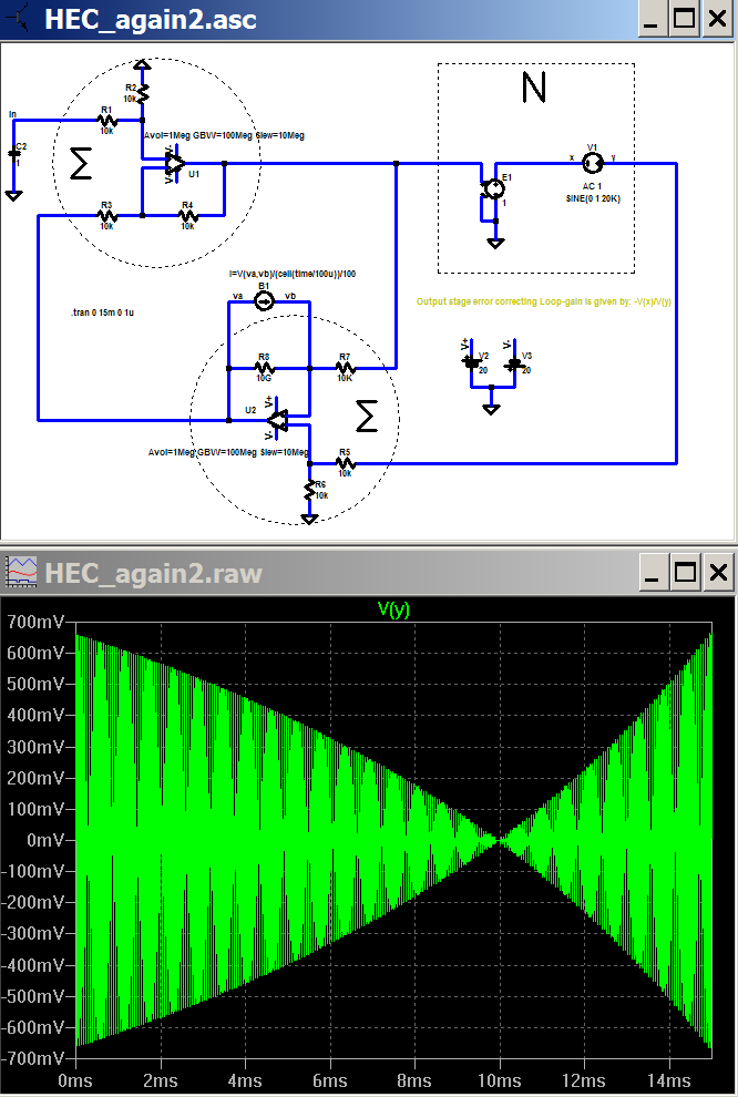
the null in the error output from V1 10KHz sine is easily visible
I really can't see what is left to demonstrate to show that "EC" is negative feedback, Mikeks originated the example circuit but persisted in making claims that I simply could not parse as fitting into the above simulation or analysis (speaking of the Spanish Inquisition...)
correcty done "model reference" control analysis should show equivalant results to the Bode sensitivity result above, but I believe there are more pitfalls in the less used approach of Hawksford that has caused much confusion - and sloppy use of "error" without distinction beween "modelling error" and "error signal"
That's all impeccable, jcx. I'm keen to help the penny drop for Jan. I think we are close. It's a confusion about how feedback is measured that is leading to the erroneous view that feedback only exists in the presence of an output error. Or something like that. And that "Hawksford EC" cancels errors out without relying on infinite feedback. Cancelling errors is a feed-forward concept.
It seems to me that it would help to show Va as a function of this same ramp.
Does it actually null perfectly, to zero, that is jcx? I think it is you who has pointed out the limitations of finite bandwidth in real hardware, which I agree is a consideration however, it seems that Bob's design shows that finite bandwidth is not a serious limitation at least in his real world design.
Pete B.
jcx said:Trimming of the loop gain is simulated below by B1 behaviorial source simulating a time dependent resistance controlling the gain of the U2 sum, B1 ramps at 100 Ohms/100 uS giving 10K at 10 ms
the null in the error output from V1 10KHz sine is easily visible
I really can't see what is left to demonstrate to show that "EC" is negative feedback, Mikeks originated the example circuit but persisted in making claims that I simply could not parse as fitting into the above simulation or analysis (speaking of the Spanish Inquisition...)
correcty done "model reference" control analysis should show equivalant results to the Bode sensitivity result above, but I believe there are more pitfalls in the less used approach of Hawksford that has caused much confusion - and sloppy use of "error" without distinction beween "modelling error" and "error signal"
you can reason backwards from the near complete null of Vy with balanced feedback resistor values to see that Va must be very nearly -Vy to accomplish the null
the exact value is determined by the limited gain available to achieve a perfect inversion in summer U1 at the frequency of the test/error source V1, of couse U2 limited open loop gain also limits the depth of the null == Error Correction
Va – V(y,x) = 400 uV in the above sim
the loop gain equation
1/2 * (a1 * a2) / (2 + a1 + a2)
gives a quite satisfying limiting case; when you consider one of the summer gains to be infinite, then the loop gain becomes
1/2 * a
when the feedback resistors define exactly canceling positive/negative feedback in the local summer and larger positive feedback loop involving both summers
my interpretation is that the null occurs at the exact feedback resistor balance that allows the positive feedback to cancel the local feedback of "a(jω)" making the maximum of a(jω)'s open loop gain available to the "error correction" loop as negative feedback loop gain
this means that EC gain is strictly limited by the gain of the circuits implementing the summers, and that the inherent negative feedback limits of how much gain can be applied are still in force - doubly so since the local EC loop is still embedded in the larger amplifier' negative feedback loop which adds its own unavoidable excess phase shift/phase margin requirements
Attachments
- Home
- Amplifiers
- Solid State
- Bob Cordell Interview: Error Correction