Hartono,
like 0.7Vrms - XVrms. Not for microphones.
We made huge set of listening test to compare BJT-JFET-MOSFET input stages.
like 0.7Vrms - XVrms. Not for microphones.
We made huge set of listening test to compare BJT-JFET-MOSFET input stages.
For 2Vrms (like CD output), this is no problem. Try them, this is the only advice. Try them and you may be surprised by sound result ... 😉
john curl said:Wow! You folks know how to 'dance' around a design problem! ;-)
I did NOT say that bipolar transistors cannot be quiet. In fact, if you took my patented design and used the very quietest bipolar transistors available today, the input noise might be as low as .2nV/rt Hz.
However, I used the quietest devices that were known at the time, and 'only' got .4nV/rt Hz back in 1973. Yes, 1/3 century ago!
With a very low impedance input, the very best bipolar transistor always has a slight advantage, BUT the FET will win over a wide range of input impedances, and this can be useful with amps and preamps of all kinds to keep the input stage quiet. Does anyone know why?
Hi John,
I agree. I think the relative absence of input current noise with the JFETs is what makes them more universal with different impedance situations.
I've never done an MC head amp, but I'd guess you can get very low input referred noise voltage by paralleling several JFETs, running them with a decent amount of standing current, and going complementary. I'm a little rusty on noise theory, but I think for a FET the equivalent input noise resistance is equal to 1/gm (I could easily be off by a factor of two). So, if you ran a standing current of about 10 mA, and got a gm of 0.04S for the group, that would correspond to a noise resistance of about 25 ohms. Then the parallel combination of the two complementary groups would cut it in half to about 12.5 ohms.
I would also think that the higher JFET immunity to RF that Nelson mentioned would be a benefit in an MC application.
Cheers,
Bob
Bob, you are slightly off in your rough calculation. As I stated before: Fet noise is related to 2/pi or about 2/3 (1/Gm).
Transistor second stage Shot noise is: .5 (1/Gm) = Req
This makes the transistor slightly lower noise with equal Gm and a lot better with a fixed operating current, such as 1ma, as you would have to use about 10ma to get a fet to have the same Gm.
You will find that my patented input circuit is quieter than almost any other, direct coupled at both input and output and operates at virtually the lowest power of any other equivalent noise input stage.
In fact, my input stage will work from a single mercury battery. However, this is impractical and not recommended.
PMA said:Christer,
sonically it is the best solution for link levels!!
Interesting. If so, then one really wonders why they are so seldom used? I can't even remember seing them at the input of any of your designs. But maybe I'm suffering from amnesia? 🙂
John,
You often seem a bit obsessed with noise. There is nothing wrong with that, and I have learnt important things about the theory of noise from you. However, I think not everyone considers ultra-low noise such a high priority for line-level signals as you do. Peoples mileages probably vary a lot here. That said, I am sure I am not alone in applauding your skills in low-noise design.
BTW, does anybody else emember John Fassottes phono amp using 16 (I think) OPA627 in parallel at each input. 🙂
john curl said:You will find that my patented input circuit is quieter than almost any other, direct coupled at both input and output
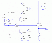
It was most interesting to have a look at this circuit as it is almost exactly what I did for a tape PB preamp circuit about 1980 without any knowledge of your patent. Unfortunately available for me at the time soviet types of transistors were pretty poor quality. Here is a fair representaion of that old circuit
Cheers
Alex
Attachments
Don't worry, you are in good company. By 1980, Ortofon had ripped me off bigtime, Michaelson and Austin made a unit in GB, and even Quad had some sort of version. Etc, etc. No more patents! Waste of my time. However, it might be more understandable why I don't publish here my detailed schematics, more often.
john curl said:Mosfets are noisy! I can't explain why, but they always are very noisy, due to 1/f noise.
John,
Indeed, MOSFETs are among the solid state devices with the largest 1/f noise. The origin of the 1/f noise in MOSFETs was throughly investigated, using both empirical equations (the so called Hooge equation) in an channel mobility fluctuation model and also using an interface charge trap model. The interface charge trapping model is largely accepted today. It predicts that the 1/f noise is mostly independent on the bias condition, inversely proportional to the square of the gate specific capacity (which in turn is inversely proportional to the gate oxide thickness) and inversely proportional to the W*L geometry of the channel.
While I would myself advise against building an input stage using discrete MOSFETs, it is a common misinterpretation that (e.g.) MOSFET op amps are "noisy" and "improper for audio". Modern technologies can integrate MOSFETs with extremely thin gate oxides and very large W*L products. These technology advances make CMOS op amps extremely competitive even in the high end audio space. Take the TI OPA365 CMOS op amp... According to my measurements, this op amp has a THD lower than 1ppm at every frequency in the 20-20k range in a 80k bandwidth, at an output voltage swing of +/-1.5Vvv and a gain of 10. The only issue with this device is the supply range of max +/-2.5V. Otherwise, performance wise, is competitive to any modern bipolar or bifet op amp, including the acclaimed LM4562, AD797, etc...
Staying slightly off topic, in the field of device technology, I'll take this opportunity to discuss here the gm drop in the IRF P channel vertical MOSFETs earlier reported by Nelson Pass. The common reason for such a behaviour is the channel trapping in the silico/silicon dioxide interface traps. Interface charges and charge traps are unavoidable in MOSFETs. These traps are simply modelled as allowed energy levels in the silicon band gap. In a very simple trap model, each such energy level has also an associated time constant. Normaly, the gate voltage controls the charge in the device channel. As long as the gate voltage frequency is low enough, the channel happily exchanges charge with the interface traps. Now, if the trap concentration is high enough and the gate voltage frequency rises, depending on the associated time constants for each energy level, some of the interface traps can't keep track of the voltage changes and fail to exchange charge with the channel. The carrier concentration in the channel decreases and hence a drop in gm as the frequency increases. To address two legitimate questions:
a) Why is this happening? Intrface traps are notoriously an issue for P channel devices, both because of the silicon/silicon dioxide interface properties but also because of the natively lower mobility of the charge carriers (holes) in the channel. However, the today's technology advances should easily avoid such issues. Assuming that IRF properly controls the IRF9240 manufacturing process, what's left is some specific switching devices manufacturing process steps. E.g. I recall irradiation and heavy metal doping in bipolar switching devices as having a very significat impact on silico/silicon dioxide inteface traps.
b) Is this a drop in gm at high frequencies or is it a boost in gm at low frequencies. I had the opportunity to crack open a few IRF9240 and, given the catalog device data and the chip properties (mainly the channel geometry and the gate oxide thickness) at low frequency the IRF9240 exhibits a holes channel mobility of about 300cm^2/V*sec. This value is to be expected for such power devices, and is within the normal range of degradation from the bulk mobility value of 450cm^/V*sec. Obviously, the gm values at higher frequency lead to much lower equivalent mobilities, which are out of the normal range for power devices.
syn08
syn08 said:While I would myself advise against building an input stage using discrete MOSFETs, ...
Since you obviously has a lot of knowledge about the physics of MOSFETs and voluntarily shared a lot of it with us, perhaps you could at least give us a hint at why you made this claim? Maybe it was just me failing to see it, but I couldn't see that this was an obvious conclusion from anything you said.
Hartono said:noise, matching
edit: capacitance removed, only if using power device.
Noise: Yes, but he specifically said the reason was not noise (although I cut that out in the quote). I am also under the impression that PMA did not consider that a problem either (I am assuming we are talking line level signals now, not phono etc.).
Matching: Do you suggest the spread is even much worse than for JFETs?
Capacitance: Well, I though of that, and that might perhaps be an issue also for small-signal devices? I only briefly checked the datasheets for a few models that are easy to get here, but capacitance seemed slightly higher than for BJTs and JFETs. Nothing extreme, though, so in most cases it probably shouldn't matter. Then we have the plateau behaviour of the gate charge, which could perhaps be an issue if not biasing sufficiently below or above this area.
Christer said:
<snip>
perhaps you could at least give us a hint at why you made this claim? Maybe it was just me failing to see it, but I couldn't see that this was an obvious conclusion from anything you said.
Indeed, it's not obvious, but otherwise very simple: current discrete mosfets are far away from the noise performance of the highly integrated MOSFETS, as used in linear ICs. Gate oxide thickness, W*L, etc... are order of magnitudes from what you can find in integrated devices. Main reason for this is that discrete devices are designed to handle relatively high voltages, both Vds and Vgs. This translates in thick gate oxides and low W*L (limited by the chip area and punchthrough effects) which in turn have a very significant negative effect on the 1/f noise performance.
Take a look to a typical discrete MOSFET like 2N7000. Vds max is 60V, while Vgs max is 20V. Compare these values to the highly integrated devices as in OPA635.
Someday a company may decide to manufacture discrete MOSFETs with performances close to the integrated devices and optimized for audio applications (beyond the intrinsic device, there are other noise mechanisms involved, like the gate polysilicon resistance, etc...). Until then, the current MOSFET devices are not ideal for very low noise applications, unless their extremely high input impedance makes them a necessary evil.
syn08
Syn08,
I must have misunderstood you earlier. I got the impression that the high noise was not the reason for your claim.
Anyway, it was interesting to learn about how the noise correlates to those variables you mention. I suppose even a 25 V Vds 0.35 W device would be very noisy then, compared to the ones in an IC.
syn08,
Thanks for your detailed discussion of the origin of the IRF P-channel transconductance anomoly. Very interesting reading!
Cheers,
Bob
Thanks for your detailed discussion of the origin of the IRF P-channel transconductance anomoly. Very interesting reading!
Cheers,
Bob
Hi Christer,
Spread seems even higher than Jfet , noise is much worse in when used in input of amplifier with large global NFB (Power amp, pre-amp). If used as follower only, the figure is much better.
Hartono
Spread seems even higher than Jfet , noise is much worse in when used in input of amplifier with large global NFB (Power amp, pre-amp). If used as follower only, the figure is much better.
Hartono
john curl said:Glen, why is Estuart's contention that your input stage is always balanced with respect to input stage gain in the complementary device pairs, bogus? Hint: Think servo. ;-)
Good day Mr Curl,
"Bogus"? Why? What do you mean?
Anyhow, the gm of the NPN and PNP LTP can be held much better under control by just keeping both tail currents equal.
"Think servo" ? What kind of servo? Normally, this term is associated with a DC control loop that keeps the offset voltage near zero,
or do you really mean a AF common mode control loop that keeps the current of both VASes under tight control? If that's the case, I can tell you that I have already recommended such loop, see:
http://www.diyaudio.com/forums/show...u can persuade him to do so. Cheers, Edmond.
estuart said:
<snip>
I have already recommended such loop, see:
http://www.diyaudio.com/forums/show... special issues I should take care of? syn08
MOSFET and BJT Inter-electrode Capacitances
We often hear concern expressed about the gate capacitances of MOSFETs. However, to put this in perspective, we really need to compare those capacitances with the analogous capacitances of BJTs.
The capacitances at issue are gate drain capacitance (Cgd) versus collector-base capacitance (Ccb), and gate-source capacitance (Cgs) versus base-emitter capacitance (Cbe).
All of these capacitances are a function of voltage, so we need to keep that in mind, but nevertheless some interesting comparisons can be made.
Here I'll compare the IRFP240 and IRFP240 with the fast Sanken RET 2SC3264 and 2SA1295.
At roughly the same collector-base and drain-gate bias, we get the following for Cgd and Ccb:
IRPP240: 300 pF
2SC3264: 250 pF
IRFP9240: 210 pF
2SA1295: 500 pF
So we see that the capacitances are comparable in this case.
For Gate-source and base-emitter capacitance we have to dig a little deeper. For example, we must take ft into account. Here we will do some hand-waiving and approximation, but that lends insight.
For a bipolar, to first order, Wt = gm/Cpi, where Wt is the radian transition frequency (ft/6.28) and Cpi is the hybrid pi capacitance. By far the biggest component of the hybrid pi capacitance is Cbe, the capacitance we are here concerned about. Thus, to first order Cbe = gm/Wt.
Now some of you may have wondered why the ft of a bipolar transistor often falls as collector current falls. The answer lies in thinking of Cpi as consisting of two capacitances.
The first, the junction capacitance, is the nonlinear capacitance we know of with a transistor or diode junction. It varies fairly slowly with the reverse voltage on the junction. Think of it as being a capacitor whose plates are spaced by the distance of the depletion region, recognizing that the size of the depletion region grows with increased reverse bias. Recognise also that the depletion region is still somewhat depleted for small amounts of forward bias on the base, where the transistor has not yet turned on by any significant amount. So at very low collector currents, Cpi is dominated by this somewhat fixed junction capacitance.
The second capacitance is the result of the transistor being turned on and the presence of minority carriers. It rises almost directly in proportion to collector current. Since both this capacitance and gm rise with collector current, and since Wt = gm/Cpi, we see that if this were the only capacitance, ft of the transistor would be constant with collector current.
As collector current falls, the relatively fixed junction capacitance begins to dominate, causing ft to fall. If one takes several points on the Ft vs Ic transistor curve, one can estimate approximately what these two capacitances are separately.
For example, while the 2SC3264 has an ft of about 50 MHz at Ic = 1A, it has an ft of only 5 MHz at an Ic = 20 mA.
Although it is certainly not the biggest constituent of Cbe at moderate currents, it is interesting to compare this junction capacitance (we'll call it Cbej) component to the gate-source capacitance of the MOSFET. The latter also changes fairly slowly with increased Id. These are the capacitances that one will see at very low Ic or Id.
2SC3264: Cbej = 23,000 pF
IRFP240: Cgs = 1250 pF
2SA1295: Cbej = 21,000 pF
IRFP9240: Cgs = 1090 pF
One can see that this capacitance is in fact much larger for the bipolar devices.
For completeness, the component of Cbe that is a direct function of collector current is shown below for the bipolars at Ic = 1A:
2SC3264: C = 0.10 uF
2SA1295: C = 0.18 uF
Finally, in fairness to the bipolar, we recognize that in a source follower or an emitter follower, these capacitances are bootstrapped by the the signal swing at the emitter or source. The factor by which the bootstrapping reduces the capacitance is greater in this situation with greater gm. Therefore, the higher gm of the bipolar mitigates these capacitances to a larger degree.
Cheers,
Bob
Bob,
Terrific post, many thanks, learned a lot.......
I must admit I like bipolars because of their high transconductance and very good rail efficiency. The SOAR issues are a major PITA, though improving with every new generation.
Cheers,
Hugh
Terrific post, many thanks, learned a lot.......
I must admit I like bipolars because of their high transconductance and very good rail efficiency. The SOAR issues are a major PITA, though improving with every new generation.
Cheers,
Hugh
- Home
- Amplifiers
- Solid State
- Bob Cordell Interview: BJT vs. MOSFET