estuart said:
<snip>
Hmm.... very strange. Can you reproduce it by means of simulation, so I can also have a look at it?
Regards, Edmond.
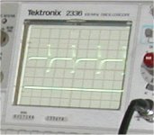
Unfortunately simulations do not show this effect. The low frequency oscillation was slightly correlated with the bypass capacitor in the reference voltage for the current sources (C4 in Glen's original schematic). Removing C4 would increase the oscillation frequency by a factor of 5, while increasing the value to 220u slightly decreased the frequency. The compensation network has absolutely no effect on this latchup/oscillation. After the latchup/oscillation occurs, removing the input signal has no effect, only powering down/up resets the circuit. That's all I tried before clamping the thing on all sides 🙂
syn08
Do you have antisaturation diodes at VAS ?
including those from VAS to lower volatge rails?
where is schematic?
including those from VAS to lower volatge rails?
where is schematic?
john curl said:Bob's post is misleading. The bootstrap capacitance must be properly computed, before it makes any sense.
John,
Please be more specific. I did point out the need for considering the increased bootstrap effect in bipolars due to the higher gm.
Perhaps you can plug in some numbers to illustrate where I am misleading.
Also, the bootstrap effect is not relevant to the Cgd and Ccb capacitances.
Cheers,
Bob
syn08 said:
Bob's post is essentially correct. Defining the BJT junction capacitances as the sum of a space charge capacitance and a diffusion capacitance is the canonic approach in the Gummel Poon model.
Computing the two capacitances is almost impossible, due to the lack of essential values like the junction exponential factor, the transit times, transport saturation currents, etc... However, if one would measure C(V) of the B-E and B-C junctions, all these parameters could be extracted and allow a fair comparison between various BJT devices. See the excellent HP paper on this topic
http://eesof.tm.agilent.com/docs/ic...MODELING/3TRANSISTORS/1GummelPoon/GP_DOCU.pdf
What I would disagree on is making this a basis to compare BJT to MOSFETs. There is no common physical model that would allow us to compare their intrinsic parameters, simply because the physics beyond the two devices is different. Perhaps a generic Hij or Yij quadripole model would allow a basic comparation. But then the quadripole models are essentially linear, a very rough approximation at the high injection levels like in an OPS. And Hij does not reflect explicitely any bias (and hence gm) dependency.
syn08
Thanks, syn08. I agree, extracting the capacitances is not easy, and comparing those aspects of MOSFETs and bipolars is difficult because they are intrinsically different devices.
My main point was that the capacitances of MOSFETs, when viewed in the proper light, are certainly no worse than those of a bipolar.
Cheers,
Bob
syn08 said:
Edmond,
I have just completed the preliminary evaluation of your design as in #1207 and I am quite dissapointed on the distortion performance. While the circuit simulates amazingly well in PSPICE, I have a breadboarded version here (with all precautions, star ground circuit, etc...) using 2N5401/2N5551 and 2SB649/2SD669 that I can't get a THD-20 under 0.01%. I have experimented with the multitude of poles and zeroes in your design, from marginally stable to a large phase margin, withouth much success in terms of THD-20.
Using the same breadboarding approach and the same bipolar devices I was able to easily bring Glen's design to a THD-20 under 10ppm, by adjusting the two pole compensation.
Things are still under evaluation, however it seems to me that, for whatever reason, your circuit has a "fighting VAS" issue. Have you implemented your design? Any special issues I should take care of?
syn08
Just curious as to the nature of the distortion?
Was this independent of signal level?
Are your referring to Glen's 12W amp in your comparision?
I only looked at Edmond's circuit quickly but noticed that each
FET is driven by a push pull follower. As far as I can tell those
followers are operating in class B, was that the intent? I have
not run the simulation, even so I would want to understand the
intent of the design.
I would keep an eye out for oscillation in the cascoded VAS, as
you probably already know.
Pete B.
darkfenriz said:Do you have antisaturation diodes at VAS ?
including those from VAS to lower volatge rails?
where is schematic?
That is precisely how I clamped the thing. The schematic is on Glen's web site, unfortunately it seems to be down now. What is strange is the combination of latchup and low frequency oscillation.
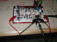
I've found this morning Glen's input stage and VAS on a breadbord, removed the clamp diodes, quickly wired and powered it up at +/- 30V and got a few shots (to follow) to illustrate the latchup/oscillation effect.
syn08
aah some people picked up the rf-thing! 😉
regarding capacitance something else came into my mind...
assuming same source resistance from the driver stage and same capacitance, wouldn't the bipolar have a smaller time constant?
I guess the b-e resistance must lower the source resistance seen by the base? 😕
regards
regarding capacitance something else came into my mind...
assuming same source resistance from the driver stage and same capacitance, wouldn't the bipolar have a smaller time constant?
I guess the b-e resistance must lower the source resistance seen by the base? 😕
regards
PB2 said:[snip]
I only looked at Edmond's circuit quickly but noticed that each
FET is driven by a push pull follower. As far as I can tell those
followers are operating in class B, was that the intent? I have
not run the simulation, even so I would want to understand the
intent of the design.
I would keep an eye out for oscillation in the cascoded VAS, as
you probably already know.
Pete B.
Hi Pete,
I think you are referring to an other design of mine, not the one depicted in post # 1207, rather
http://www.diyaudio.com/forums/showthread.php?s=&threadid=94676&perpage=10&pagenumber=92 post #912.
Any how, the intent is that the followers are operating in class-AB. Using four transistors might look a waste of silicon, but it isn't, as each of them has to deliver only half of the current to the gates. So they can have half the size of drivers that would be needed in case of using only two transistors. Besides, this topology allows better control of the turn-on/turn-off delay of the MOSFETs.
Oscillation in the cascoded VAS? If you expect oscillations, please tell me more about it.
Cheers, Edmond.
Hi all
Sorry, I've missed quite a bit of this discussion. Backing up a little - surely gm doubling (or not) depends on the impedance which is driving the output stage.
In an ideal current source, both transistors being on cannot have gm doubling distortion. In this case "gm" is an inappropriate measurement since current is multiplied. Reason is simple: if current splits into one output half, it cannot go into the other. Thus if two stage halves in the output have a current gain of 100 and they're both on, 1 mA excursion in the VAS will split (if the impedances are matched) to 0.5 mA each and you have 50 mA out x2= 100 times = same as one half being on. If the impedances are mis-matched (say due to one side approaching cut-off) the current still divides and the output is still the total of both pieces. No "gm doubling".
On the other hand Miller-VAS's and most practical VAS configurations cannot achieve the ideal current drive. As soon as the ideal situation is not achieved, then some form of gm doubling is going to occur, because now we are dealing with some impedance rather less than infinity. But the higher the impedance can be maintained, the better is the transfer characteristic. Another reason, incidentally, why it is better to try to avoid hanging capacitors onto the VAS collector.
It is possible to build amps without capacitors on the VAS, but usually this has to work with lower overall gain. Crossover distortion is virtually absent (indicated by reducing harmonic levels) and the net distortion is in the 0.0x % rather than 0.00x% league.
cheers
John
PB2 said:
Just curious as to the nature of the distortion?
Was this independent of signal level?
Are your referring to Glen's 12W amp in your comparision?
I only looked at Edmond's circuit quickly but noticed that each
FET is driven by a push pull follower. As far as I can tell those
followers are operating in class B, was that the intent? I have
not run the simulation, even so I would want to understand the
intent of the design.
I would keep an eye out for oscillation in the cascoded VAS, as
you probably already know.
Pete B.
It was almost independent on the signal level, but was frequency dependent, and 0.01% was at 1KHz. At 20KHz it was almost 0.08%. Yes, I'm comparing with Glen's 12W design.
I would expect a cascoded VAS to occasionally oscillate, but not at 3KHz...
syn08
syn08 said:
It was almost independent on the signal level, but was frequency dependent, and 0.01% was at 1KHz. At 20KHz it was almost 0.08%. Yes, I'm comparing with Glen's 12W design.
I would expect a cascoded VAS to occasionally oscillate, but not at 3KHz...
syn08
Hi syn08,
0.08% is 1000 times!!! the simulated THD20. Something must be terrible wrong. Did you received the high res. drawing and find any discrepancy?
Regards, Edmond.
estuart said:
Hi syn08,
0.08% is 1000 times!!! the simulated THD20. Something must be terrible wrong. Did you received the high res. drawing and find any discrepancy?
Regards, Edmond.
I haven't got the drawing yet. BTW, the bias points simulated and measured were in the +/- 5% range.
Thanks,
syn08
syn08 said:
I haven't got the drawing yet. BTW, the bias points simulated and measured were in the +/- 5% range.
Thanks,
syn08
Huh? I have sent it more than four ours ago!
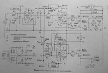
Why is this method not popular? 1 transistor (bipolar/mosfet) is driven by 1 opamp, we can get very high impedance input of output stage with very low output impedance. (won't load the VAS so much that the loading will cause distortion of VAS output while the emitor/source node will be corrected by the opamp towards the input of the opamp)
Look at the upper OPA627 driving BUZ21 in follower mode.
Floating +/-15V can be made by simple bootstrapping towards the output node.
Look at the upper OPA627 driving BUZ21 in follower mode.
Floating +/-15V can be made by simple bootstrapping towards the output node.
Attachments
estuart said:
Hi syn08,
0.08% is 1000 times!!! the simulated THD20. Something must be terrible wrong. Did you received the high res. drawing and find any discrepancy?
Regards, Edmond.
Do not believe simulations much. THD simulations sometimes fit, sometimes absolutely not.
syn08, I am sure you have checked PCB or breadboarding, especially NFB return point (physical placement).
- Home
- Amplifiers
- Solid State
- Bob Cordell Interview: BJT vs. MOSFET