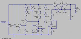
Twitchie, I would suggest replacing that LM334 with Martin's CSS components (on post 184) and adding the emitter resistor to the shunt transistor Q1 to actually measure the shunt current. There seems to be a remarkable reluctance to add the seperate tracks for best performance, despite repeated advice from Jan and others - it goes like this, on the cct above...From Q7 collector, track to shunt Q1 (+ Led3) then to the o/p terminal OUT-1 (+V) - this (OUT1) terminal has a further 3 seperate tracks for C3 &R4, another for Led1 &R6, and the C2. So the OUT-1 has 4 tracks On the 0volt line, ideally, there are 6 seperate tracks for nearly everything - the C1, the LM334 (or replacement), D3 & C4, R3, R1 &Q1 emitter, the C2, all going to the O/P terminal OUT-2 (0V)
janneman said:Right. Then I suggest to replace it with a zener symbol....
Jan Didden
D3 as well
First iteration generated from schematic:
Changes;
- CCS'ed
- some pseudo ground tracks added
- Q1 emitter resister added
- got rid of yet another jumper (down to 1)
- zeners in place of D1 and D3 (I think it's right, but could be wrong)
Schematic:

Board:

Changes;
- CCS'ed
- some pseudo ground tracks added
- Q1 emitter resister added
- got rid of yet another jumper (down to 1)
- zeners in place of D1 and D3 (I think it's right, but could be wrong)
Schematic:
Board:
twitchie said:First iteration generated from schematic:
Changes;
- CCS'ed
- some pseudo ground tracks added
- Q1 emitter resister added
- got rid of yet another jumper (down to 1)
- zeners in place of D1 and D3 (I think it's right, but could be wrong)
Hi twitchie,
It looks like you are doing a good job. 😀
I would have another look at your pseudo ground tracks, seems like the positive rail to me.
regards
Hi,
the multiple trace routes on the line side should be repeated on the return side.
If LED1 & LED2 work for the CCS on the shunt side , then why change to Zener and diode for the input CCS?
The BF245 can be different grade. The lower can be grade A and the upper can be grade B or C. The voltage across the lower device must be at least double it's pinch off voltage. A resistor in the source to trim a B device will not achieve that voltage criteria. A low pinch off voltage device must be used. Grade A moves in the correct direction, k170 will be even better.
R10 is far too high. It forces Q2 to do most of the work.
Which resistor(s) do we want to use for adjusting voltage? I had the pot at R8 (LM334 resistor), but thanks to an email from a kind member (thanks BDP) and some reading on "Shunt Regs for Dummies", I see the voltage divider R3/R4 (tell me if I'm wrong please)
Can we also make the current adjustable? (R9?)
- leds replace zener/diode on CCS input
- final jumper can be omitted with a bit of LED leg stretching
Can we also make the current adjustable? (R9?)
- leds replace zener/diode on CCS input
- final jumper can be omitted with a bit of LED leg stretching
An externally hosted image should be here but it was not working when we last tested it.
Great work… there seems to be space to move LED1 pads just where the jumper pads are so no need for stretching leads.
Whats the actual size of the board?
Whats the actual size of the board?
Thanks Tony 😉
I was going to modify the footprint of that led to have stretched legs, but haven't had the chance yet. It's a bit more work than just adjusting the footprint because all the other leds share the same package (same part)
This layout is still tied to the schematic, but my plan was to take a copy of the .brd and hack it before etching (adding pads and moving LED1 as you already picked up on)
The board in it's current state is pretty much the same size as the pre-Jan version give or take a millimetre or 2. I have one I etched from your files (or was it Manu's) that I used to compare against.
Eagle says it's 2.4x1.625 inches
I was already giving up hope that this was moving in the right direction but thanks to twitchie it now does 😎 . One suggestion that I continue to make is to use two LEDs instead of 1 for LED3 (will not cost more board space). Otherwise you have to use a different LED with higher forward voltage in this position (potentially more noise) AND limit yourself in the resistance range of R2 and hence the loop gain.
I have my own suspicions. When testing another CCS in LTSpice I noticed that the current was less than 10% of the calculated value with the default LED model of LT Spice. This was a result of the forward voltage being way too low. With a proper LED model I now get correct forward voltage and current in my CCS - I "presume" whoever played with this in simulation ran into similar problems and chose a new voltage source to solve this.
P.S. In my original simulations the performance of the regulator was somewhat "immune" to component changes (e.g. C3 and C4) but now I do get better results.
then why change to Zener and diode for the input CCS?
I have my own suspicions. When testing another CCS in LTSpice I noticed that the current was less than 10% of the calculated value with the default LED model of LT Spice. This was a result of the forward voltage being way too low. With a proper LED model I now get correct forward voltage and current in my CCS - I "presume" whoever played with this in simulation ran into similar problems and chose a new voltage source to solve this.
P.S. In my original simulations the performance of the regulator was somewhat "immune" to component changes (e.g. C3 and C4) but now I do get better results.
It's good to see you chime back in as well MRupp and I had a sneaking suspicion that we would eventually be gravitating back to your schematic in post 184, so the current schematic and layout I have in front of me has 2 LEDs where LED3 currently resides 
Now does anyone have any input on which resistor(s) to change to pot for adjustments? It might be a bit of a struggle to change R4 to a pot, so if adjustment is supposed to take place somewhere else, that would be good to know.
I'm sure everyone would like to see this finally put to rest (or copper and fiberglass
  )
)
Now does anyone have any input on which resistor(s) to change to pot for adjustments? It might be a bit of a struggle to change R4 to a pot, so if adjustment is supposed to take place somewhere else, that would be good to know.
I'm sure everyone would like to see this finally put to rest
(or copper and fiberglass )Maybe asking too much but R10 seems in a rather odd position couldn’t you push the power tranies to the edge a bit and drop the resistor to a lower position? Otherwise looking very good.
Cheers
Cheers
Simulations
For those who are interested in simulations: A better LED model for LTSpice can be found in "Analyze LED characteristics with PSpice" by Sam Mollet: http://www.edn.com/contents/images/11801di.pdf
The model that I am using now is in figure 2 and this seems to give much better results.
For those who are interested in simulations: A better LED model for LTSpice can be found in "Analyze LED characteristics with PSpice" by Sam Mollet: http://www.edn.com/contents/images/11801di.pdf
The model that I am using now is in figure 2 and this seems to give much better results.
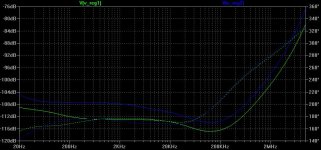
Here is an example showing load regulation, with 5mA AC load current and 50 mA DC load current, Vin AC component to 0 Volts. The green line is with C4 = 220uF parrallel to the voltage reference, the blue line has C4 = 4.7uF. This seems to give a small improvement of ca. 5 dB. This is not much but in my previous simulations these changes did not do anything to the performance which shows that the simulations where not working because the regulator was current starved:
Attachments
- Status
- Not open for further replies.
- Home
- Amplifiers
- Solid State
- Bipolar discrete shunt regulators