Stability is an important parameter for an amplifier, but at what cost? Still, I wanted to boost the open loop by more than 100 dB and a higher frequency pole.The oscillation is gone.
this R11 needs to increase the denominationOver load recovery is not good.
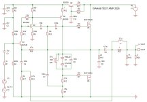
This is my final take on this amp.
I had taken the original amp, from post #1, adjusted the olg as per Bonsai's post and the tutorial of minek, and posted it in post #15. I posted the final ASC in post #18.
Then, our dear friend HK (Hennady Kovalsky) made a series of suggestions. I tried to incorporate them with partial success.
Again, I had taken the suggestion of HK for a EF buffer before the outputs, but retaining the Bootstrap, I redid the exercise again. The final outcome is as below.
Only the Distortion graphs are given below.
The OLG margins, the Squave Wave output and Over load recovery are similar for both cases.
I request that the simulations I had done may please be duplicated to prove that no silly mistakes have been made.
Thanks to minek and Bonsai for starting me off on this. And HK for the new direction. The .asc files posted can be run straight away. As I am having the old version of LT, I request minek and Bigun to look at the simulation carefully.
Attachments
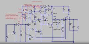
I could not implement HK's suggestion to take second FB from after the output Elec as I could not simulate the OLG correctly. I request that that variant be tried.
If C13 and R21 are removed, the Dis profile improves.

If C13 and R21 are removed, the Dis profile improves.
Attachments
Last edited:
Please wahab, I would like to hear from you!100R for the TMC network is way way too low, try with a higher value, in the meantime i ll post my take on this kind of design later.

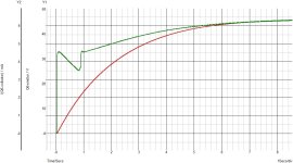
With the help provided by wahab, entered into LTspice the circuit details. The .asc file is attached. I shall be posting my test graphs shortly. Quick check shows good SQwave responce, with and without cap parallel to LS. Over load recovery is also neat.
Attachments
Last edited:
Quick check shows good SQwave responce,
- I propose to reduce the nominal value of capacitance C3 to 22 µF - this will facilitate the operation of the charge-discharge current filter for Q4.
- in order for the input resistance to be more linear, it is necessary to increase resistor R4 and proportionally reduce R3, while increasing the value of capacitance C4 to 100 μF, because the capacitance rating of this capacitor C4 must be at least 10 times greater than the input capacitance C1.
Tau1= R4(75k)*C4(22uF+/-10%)= 1.65s
Tau2=R4(15k)*C4(100uF+/-10%)=1.5s
Tau1=Tau2 (+/-10%)
Thus, changing the ratings will not affect the level of noise filtering at the power supply input of the amplifier.
Attachments
Last edited:
Hennady, if you look at the schematic i posted i use a BC639 as cap multiplier, that s not by chance, if Gennajy use a BC550
that s another story, that s not adapted for the purpose.
The 220uF cap C3 is necessary with the cap multiplier to have 100dB PSSR at 100Hz, reducing the value will degrade the PSSR.
The high value resistance, 82k in my schematic and 75k in the schematic above, in serial with the 22uF cap
guarantee a soft start for the amplifier, this way the currents in the amp will increase at a slow rate and particularly
the output cap will be charged without a big peak current through the NMOS.
Beside the cap multipler is driven through a 10k resistance that will also guarantee a low enough current to charge
the 220uF cap, in principle with all the cited value there will be no big in rush current.
Capacitor C3 with a capacity of 220 μF is suitable for this transistor.i posted i use a BC639 as cap multiplier
ask him why he installed a weak transistor?if Gannajy use a BC550
that s another story, that s not adapted for the purpose.
look at the calculation of Tau1 and Tau2, they are the same, i.e. will also turn on smoothly.in my schematic and 75k in the schematic above, in serial with the 22uF cap
guarantee a soft start for the amplifier, this way the currents in the amp will increase at a slow rate and particularly
the output cap will be charged without a big peak current through the NMOS.
The nonlinearity of the input impedance in your version is very bad for the sound. Capacity C2 must be at least 10 times greater than C1.
Last edited:
That doesnt matter since the impedance of the 22uF cap is very low in respect of a 100k resistance, and even if the cap was much smaller that would still have no effect at all other than increasing the input impedance at low frequencies, eventually if there were
no cap at all this would increase the input impedance to something like 100k, the only effect would be a little lower PSSR.
There s eventually distorsion if the transistor input impedance is not stable, and even then the negative feedback will correct
any non linearity, to say that something would sound bad means nothing if there s no evidence that distorsion is high,
that s just an opinion that is not scientificaly supported.
Wahab: 'I use a BC639 as cap multiplier'
Unfortunately, BC639 is not in the file "minek.lib'. Instead of searching for the model, I used BC550 which was available.
Unfortunately, BC639 is not in the file "minek.lib'. Instead of searching for the model, I used BC550 which was available.
For AC input voltage, this capacitor C4 is connected in series with capacitor C1. And R4 is as much as 2 times smaller than R5, so it is this circuit R4 C4 that will determine more than 50% of the nonlinear input impedance of the amplifier.That doesnt matter since the impedance of the 22uF cap is very low in respect of a 100k resistance, and even if the cap was much smaller that would still have no effect ...
It doesn't matter to you because you don't see obvious things, it's simple arithmetic.
the input circuit is outside the negative feedback loop, NFB won’t fix anything for you in this case.There s eventually distorsion if the transistor input impedance is not stable, and even then the negative feedback will correct
This comment looks very stupid...to say that something would sound bad means nothing if there s no evidence that distorsion is high,
that s just an opinion that is not scientificaly supported.
Good, you can use anything comparable but although i wouldnt advise to use a BC550 in a build it would still work without any failure, here the current and output voltage of the transistor at start up, as you can see the peak power wont exceed 0.25W for a very short duration.
And also here the spice model of the BC639, you can add it in a in your asc. folder along with the other models.
*ZETEX BC639 Spice Model v2.0 Last Revised 24/2/05
*
.MODEL BC639 NPN IS =6E-14 NF =0.99 BF =250 IKF=0.9
+NK=0.7 VAF=270 ISE=1E-14 NE =1.2 NR =0.98 BR =30 IKR=0.5
+VAR=27 ISC=1.2e-13 NC =1.2 RB =0.2 RE =0.08 RC =0.08 RCO=5
+GAMMA=5E-9 CJC=15.9E-12 MJC=0.4 VJC=0.51 CJE=108E-12
+MJE=0.35 VJE=0.7 TF =0.8E-9 TR =55e-9 XTB=1.4 QUASIMOD=1
*
*$
*
Attachments
Last edited:
For AC input voltage, this capacitor C4 is connected in series with capacitor C1. And R4 is as much as 2 times smaller than R5, so it is this circuit R4 C4 that will determine more than 50% of the nonlinear input impedance of the amplifier.
It doesn't matter to you because you don't see obvious things, it's simple arithmetic.
the input circuit is outside the negative feedback loop, NFB won’t fix anything for you in this case.
This comment looks very stupid...
I dont want to do any polemic, but either you do some sims to prove your sayings or otherwise that s just talking
out of the vaccum.
The input circuit is not outside the NFB loop in case you didnt know, the base of the device is tied
to its emitter, that s why the negative feedback increase the input impedance, so much for the stupidity
and what is obvious.
If you don't know something, then don't invent it, because the negative feedback loop implies linearity, and the connection through the emitter-base junction is nonlinear, so the linearity of the input resistance is determined by the input passive elements.The input circuit is not outside the NFB loop in case you didnt know, the base of the device is tied
to its emitter,
The smart one will understand, the stupid one will demand proof.I dont want to do any polemic,

If you don't know something, then don't invent it, because the negative feedback loop implies linearity, and the connection through the emitter-base junction is nonlinear, so the linearity of the input resistance is determined by the input passive elements.
The smart one will understand, the stupid one will demand proof.
For the time it s you who are talking of parameters that you re unable to quantize, that s just vague statements out of the wild,
but at each step you re just showing that you dont really understand your own logic, or rather lack of.
What you are talking about is the input impedance seen by the source, but this has nothing to do with the transistor intrinsical input impedance, lowering those resistances by a 10 factor not only wont change the current absorbed by the transistor base for a given output current variation but also the base/emitter resistance wont change as well, be it by a iota.
Hence the non linearity of the input device cant be improved by changing the biaising resistances values and keeping the same ratio, only in your imagination eventually, the only thing that wil change, as already said, is the current provided by the source to feed these resistances.
Wahab: 'I use a BC639 as cap multiplier'
Unfortunately, BC639 is not in the file "minek.lib'. Instead of searching for the model, I used BC550 which was available.
I ve seen that you reduced the gain by a 3 factor by setting R6 to 220R, this reduce the input stage gain, best is to reduce the two 4.7K resistance (R7/R21 in your sch) to 3.3K and set R6 to 150R, this way there will be a little less distorsion, eventually you can set R7/R21 to 3.3k and set R6 at 100R, the gain will be greater but stability will be better as well and distorsion wont increase, as implemented currently with 2 x 4.7k and 220R the gain is only 11.6x, i would think that something like 30x is more adapted to various sources.
I argued only for the linearity of the input resistance for an alternating signal, read more carefully, smart guy, but what you write is already the nonlinearity of the active element and it naturally will not go away.Hence the non linearity of the input device cant be improved by changing the biaising resistances values and keeping the same ratio, only in your imagination eventually, the only thing that wil change, as already said, is the current provided by the source to feed these resistances.
- Home
- Amplifiers
- Solid State
- "Bigun's TGM8 with single Supply" Revisited