Member
Joined 2009
Paid Member
I have since discovered that you (AndrewT) have owned the Crimson (the 1100 was the first one you bought a very long time ago) and that you might possibly be in a position to share a schematic with me ? (otherwise it looks as if Crimson is a small company with little known about their designs - the only name I can find is Brian Powell who was / is the designer as of 2006).
Another gem I was able to dig up was a schematic by Ingrast, a DIY audio member who hasn't been around for awhile - see attached for his design which at the time he was doing this had filed a patent and didn't want to disclose all the details. It appears to use some additional devices to gain enough sensitivity to monitor the output current across relatively small resistors. Of further interest is the concept of using MOSFET output devices which don't suffer from gate-capacitance charge up effects if you keep them always-on as is proposed here.
Another gem I was able to dig up was a schematic by Ingrast, a DIY audio member who hasn't been around for awhile - see attached for his design which at the time he was doing this had filed a patent and didn't want to disclose all the details. It appears to use some additional devices to gain enough sensitivity to monitor the output current across relatively small resistors. Of further interest is the concept of using MOSFET output devices which don't suffer from gate-capacitance charge up effects if you keep them always-on as is proposed here.
Attachments
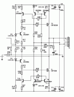

I've redrawn the top half of this output in a format that matches your description. Now I see it. Very clever - and quite fun to make the leap from your first schematic to something more recognizable. There's so much to see in this design and lots of potential for playing with it. It's possibly a novel way to look at the CFP.
You got it right. The bottom part, P-type, is a mirror reflection, and both VAS-es are loaded one on another.
You may look at it also as a Sziklai Darlington with additional diode (bottom) that protects it from over-current, and one more diode (top) that thermo-compensates an output transistor.
Last edited:
In any case, I could patent it: it is a unique topology, with own unique properties. Now, since it is in Public Domain, everyone can enjoy it, but nobody can sue me for patent law violation if I start using it commercially.
Member
Joined 2009
Paid Member
So many good ideas - when I'm back from my business trip I'm going to have to set up some simulations (haven't played with Spice for months now).
Wavebourn - patents seem to have no direct correlation with common sense, patent offices approve patents they shouldn't and companies successfully prosecute and defend patents despite glaring problems like prior art because it's just easier to settle or it maybe that another company caved in during some back room deal which sets a precedent for everyone else to get scre*ed over.
Wavebourn - patents seem to have no direct correlation with common sense, patent offices approve patents they shouldn't and companies successfully prosecute and defend patents despite glaring problems like prior art because it's just easier to settle or it maybe that another company caved in during some back room deal which sets a precedent for everyone else to get scre*ed over.
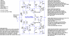
Hi Gareth, Here is an output stage I have used in Le Gecko, it is hyper linear and distortion is negligible. Simulate and see if it serves your needs. Nico
Hi Nico,
clever,
how about thermal stability?
quiescent current?
what transistors type?
offset reg with r18/19?
Nico please check

Nico
please look at the attm
something wrong: output voltage is twice lower than input voltage😕
at lower levels this thing (not the buffer) is distortionless
at 10V at the input you will get the curves like attached...
Here is an output stage ...Nico
Nico
please look at the attm
something wrong: output voltage is twice lower than input voltage😕
at lower levels this thing (not the buffer) is distortionless
at 10V at the input you will get the curves like attached...
Attachments
Member
Joined 2009
Paid Member
Nico - very nice circuit.
Well, I'm back from my business trip and it gave me time to reflect on things a bit more. I think my heart just isn't in ClassAB anymore. I took a break from things to build a SET and yet the fun of the intellectual challenge pulled me back here. But I still get the feeling that AB is not where I want to go. When I look at the compromises, the 'lumpy' gain characteristics at cross-over at low powers where I least want it, the amazing complexities if using negative feedback to correct for it - just isn't an elegant solution. As Einstein used to say, the right answer will be elegant and simple. So I'm going to leave you guys to pick up on some of the great ideas here for awhile instead of rushing in to build something myself.
Well, I'm back from my business trip and it gave me time to reflect on things a bit more. I think my heart just isn't in ClassAB anymore. I took a break from things to build a SET and yet the fun of the intellectual challenge pulled me back here. But I still get the feeling that AB is not where I want to go. When I look at the compromises, the 'lumpy' gain characteristics at cross-over at low powers where I least want it, the amazing complexities if using negative feedback to correct for it - just isn't an elegant solution. As Einstein used to say, the right answer will be elegant and simple. So I'm going to leave you guys to pick up on some of the great ideas here for awhile instead of rushing in to build something myself.
This is the best class AB stage
Hybrid Amplifier by Andrea Ciuffoli
and now I am testing this
Hybrid Amplifier by Andrea Ciuffoli
I will try soon 2sk1058 instead of BUZ900P and 6C45 or 5842 instead of D3a
Hybrid Amplifier by Andrea Ciuffoli
and now I am testing this
Hybrid Amplifier by Andrea Ciuffoli
I will try soon 2sk1058 instead of BUZ900P and 6C45 or 5842 instead of D3a
I took a break from things to build a SET and yet the fun of the intellectual challenge pulled me back here...
Hi Bigun!
almost the same reason like mine.
Just looked for "not watts sucking" good sounding ss ab buffer,
instead listening my wattsucking 5W excellent sounding SET...
anyway
maybe this thread will be continued with other clever designs?
NicoRas,
I found your design has hogh output impedance,
could you show the values used parts?
Member
Joined 2009
Paid Member
Diamond Buffer is the best AB stage? 😀
Please, don't make my slippers lough... 😉
You wear slippers, come on, it's warm in California, try living in Ontario! 😛
Member
Joined 2009
Paid Member
So Wavebourn, what do your slippers believe is the best topology if not a DB ? I believe your A + C topology uses feedback and this thread is about no-feedback Class AB. A CFP output clearly includes nfb between output and driver and I have never seen Error correction implemented for an output device without negative feedback to the driver. So that leaves EF output (which DB has at its end).
"Please, don't make my slippers lough..."
So, do you have anything useful to share with us?
Is there some fatal flaw in this design?
Andrea Ciuffoli has some good and proven designs, the cool follower being one example. You could do far worse.
So, do you have anything useful to share with us?
Is there some fatal flaw in this design?
Andrea Ciuffoli has some good and proven designs, the cool follower being one example. You could do far worse.
Member
Joined 2009
Paid Member
Margan
I couldn't resist a quick look at that Margan idea - essentially looking at the current flow at the output to determine when the devices switch off and boosting the current to Diamond Buffer to prevent it.
I'll attached the spice file (to the next post) for somebody else to play with - it's a bit of botch job, not very effective, not very stable and not clean enough.
Voltage drop is measured across a diode and the signal used to modulate the CCS that powers the diamond buffer signal stage. That's all I did.
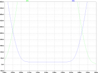
First plot is the schematic.
Second plots shows current through an output device, never turns off.
Third plot shows same thing if you get is all messed up - looks strange eh ?!
If you know how to configure this thing to work properly please let me know !
I couldn't resist a quick look at that Margan idea - essentially looking at the current flow at the output to determine when the devices switch off and boosting the current to Diamond Buffer to prevent it.
I'll attached the spice file (to the next post) for somebody else to play with - it's a bit of botch job, not very effective, not very stable and not clean enough.
Voltage drop is measured across a diode and the signal used to modulate the CCS that powers the diamond buffer signal stage. That's all I did.
First plot is the schematic.
Second plots shows current through an output device, never turns off.
Third plot shows same thing if you get is all messed up - looks strange eh ?!
If you know how to configure this thing to work properly please let me know !
Attachments

Member
Joined 2009
Paid Member
There are no emitter degeneration resistors, and unlike a JLH f.e., it operates in class B, and has room for thermal runaway.
Perhaps less than a conventional complementary PP where it can be extremely brutal, but enough to run into troubles.
The servo operates on a relatively small range, and is not sufficient to accomodate wide temperature variations.
To avoid thermal runaway without any servos and without Ube compensation - mostly realized by the use of a variable Vbe multiplier or forward-biased silicon diodes (voltage stabilizers like ZTE1,5) there is an other excellent approach: the use of emitter degeneration resistors in high impedance version. The disadvantage is here, that the available output current is sufficient only for headamps and line driver stages in preamps.
An interesting question for me is in this matter follow:
Which value of this emitter degeneration resistor is at least necessary for reliable prevention of thermal runaway, as long as no other countermeasures, sorceries and tricks therefore are in use (like Vbe or any kind of servos) ??
Which calculation steps I must know? I think, anywhere I have read about this a formula (voltage drop across resistor and Ube voltage from power devices of arround 260mV); unfortunately I don't know in the moment, where I must look.
Thank you for your support to find the associated paper.
Last edited:
Member
Joined 2009
Paid Member
You need Re > 1/gm, where gm is the transconductance, to have a resistance that will stop thermal runaway.
And it turns out that this formula also gives you what you want for optimal Class AB biassing too, where the voltage drop across Re is around 26mV.
And it turns out that this formula also gives you what you want for optimal Class AB biassing too, where the voltage drop across Re is around 26mV.
That will not necessarily stop thermal runaway: it depends on heatsink, supply, voltage, etc.You need Re > 1/gm, where gm is the transconductance, to have a resistance that will stop thermal runaway.
For runaway to occur, the gain of the loop must be >1: if an initial increase of 1W in dissipation results in a larger than 1W response, there is positive feedback.
1W will increase Tj by Rth, Tj will increase Ic by tempco/Re, and Pd will increase by Vs x Ic.
That is the somewhat simplified outline.
Being too near the limit is not recommended, as small perturbations will lead to huge delta T°'s
- Home
- Amplifiers
- Solid State
- Best topology for no-feedback ClassAB buffer ?