Onvinyl said:How about exchaning Q1 with a mosfet? You get more voltage drop for free, just add the drop the zener value. I've done it with 9610 and zvp3306 successfully in my own reg.
Rüdiger
Do you mean Q3?
ikoflexer said:Craig, I cannot agree more with you about the disparity between simulation and reality. I still do quite a bit of simulation to test out ideas, but always go to the soldering iron for a reality check.
If you feel like it, would you please comment on the circuit attached? While it is not the most extraordinary in simulation it does have good results there too. However, in reality it performs very well. (For outstanding simulation results I posted a circuit earlier, unreal, really.) Do you see any possible areas where we could improve? Thanks in advance.
ikoflexer ,
J1 R5 is overkill and seeing that semicondcutors generally operate better in linear mode when they have more optimum operating points then it is not optimal from that perspective and in this application. It can be replace by a resistor as Vbe of Q1 is relatively constant, Vbe/R = constant I.
The MOSFETS are over specified for the circuits parameters and intentions. Better performance can be gained by choosig a more suiably spec'ed part.
D8, C2 could benefit from RC filtering. You have the C there already, just need and R between D8 and C2 -ve to base Q1.
In Salas's post #255 it looks like the headroom for the current source feeding the shunt is marginal.
I feel uneasy with how the circuit balances the shunt current, but it is just a gut feeling. D8's biasing comes to mind.
I would prefer to use bipolars rather than MOSFETs.
R4 and J2 positions can be exchanged to improve what you are trying to do here. However, I see it as overkill and that the current source performance would not be degraded much by removing C1 and R4 and just using the J2 current sink. Of courxe a series R for J2 would be needed to keep its Vds in range if higher voltages are used.
J8 can be replaced by a resistor as in Salas's post #255. This ressitor will set the bias current for Q1. I.e Vgs(m2)/R(Q2)
It goes without saying that I am commenting upon a model with very few DC operating points specified. These will need to be checked and optimised.
Craig, I agree with everything in your post, except for the collector load on the main shunt amplifier. Having the JFET there as a load makes a huge difference in measured performance (which makes sense, since it greatly increases the noise gain).
In particular I agree that a CCS on the zener is superfluous.
In particular I agree that a CCS on the zener is superfluous.
I did not have it there until I saw very low frequency instability. Put the CCS under the Zener, bingo! gone!
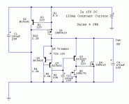
Q5, 7 cannot operate properly with only 600mV coming from Q3.
In all of these schematics, they would have better DC operating conditions if the single transistor (Q3) were replaced with a Darlington.
What would a Darlington do to the AC and dynamic performance?
In all of these schematics, they would have better DC operating conditions if the single transistor (Q3) were replaced with a Darlington.
What would a Darlington do to the AC and dynamic performance?
AndrewT said:Q5, 7 cannot operate properly with only 600mV coming from Q3.
In all of these schematics, they would have better DC operating conditions if the single transistor (Q3) were replaced with a Darlington.
What would a Darlington do to the AC and dynamic performance?
Or lift Q3 with a resistor a bit. Q5,7 they still work though.
A Darlington would either boost everything nicely or oscillate easily. I haven't put one there yet so to know if it will be stable.
based on your posted values and voltages,salas said:Q5,7 they still work though.
Q3Vbe~620mV.
Q5Vbe~610mV and
Q7Vce~10mV.
Will it work with these values? Maybe, but how well?
How much base current is passing Q7?
What effect will this have on performance?
q7 passes 0.83mA to create the 8.3Vref+0.7VbeQ3=9Vout. Base 253uA.
R6 can be scaled much lower, and by using the trimmer at lower range, double or triple the current through q7.
Not much effect I would think. Rather risking more thermal drift in the ring of 2 CCS and Vref resistor.
R6 can be scaled much lower, and by using the trimmer at lower range, double or triple the current through q7.
Not much effect I would think. Rather risking more thermal drift in the ring of 2 CCS and Vref resistor.
Hi,
how much current do you want to pass Q7, when Vce~10mV?
What is the base current of Q7 when you do this?
How much will this base current vary, as Q3 asks for more/less drive to operate the shunt regulator?
Edit.
I see you quoting 253uA IbQ7.
What effect does varying this have on the way Q5 tries to hold a constant voltage across the 1k trimmer?
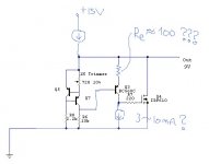

Babowana said:Could be better with Re inbetween 100R and 150R?
>🙂<
Yes Babo.
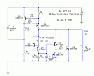
post 272 is completely at odds with post 269.
If post269 quotes Ib=253uA for Ic=0.83mA
then in post272 increasing Ic=3.1mA, must give Ib >>530uA.
If this is simulator predictions then the simulator is wrong.
I suspect it cannot model saturated transistors.
You are wasting your time trying to simulate saturated transistors.
Breadboard the circuit as a basic Q3 and compare real voltages and real currents to the versions with Q3+Re and to Darlington Q3.
I am sure about it. Real best will show on bench. Simulators aren't for such questions especially when simulating simply and fast for checking some ideas. Is it really worthy to increase the DC margin for ring of 2? Will the Darlington oscillate in a practical layout? Need different stoppers? That is why I said it must be practically tested and compared. Good thing so far is that we saw we can lift the transistor instead if there is oscillation with a Darlington, and there is practical performance gain to have more voltage bracket for the ring of 2. If JWB likes it, he may test. I devised it with him in mind, since he uses such Mosfets and has it breadboarded.
AndrewT said:post 272 is completely at odds with post 269.
If post269 quotes Ib=253uA for Ic=0.83mA
then in post272 increasing Ic=3.1mA, must give Ib >>530uA.
I think I made a mistake back then. It was about 140uA for 0.83mA, and 258uA for 1.7mA that I mixed up.
still does not compute.salas said:.... It was about 140uA for 0.83mA, and 258uA for 1.7mA that I mixed up.
hFE comes out at 5.93 and 6.59. Too high, if Vce=0.01Vce and in the wrong ratio. Beta droop as Ic rises, particularly at very low Vce.

- Home
- Amplifiers
- Power Supplies
- Best low noise regulator?