Others please check / verify!
Andy, if it makes it easier for you to get the probes where they need to be... Here is what I did.
I was fortunate to have 3 DMMs, but only 2 sets of probes I could fix with hooks across R10 and R11.
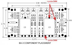
So, I put the two fixed sets across R10 and R11 to measure bias. I installed a large cap in the "big" location for C3. Getting a probe to the "top" point on R12 (on the C3 side) was tight, and it was also too tight for me to get a probe to the "top" side of the big C3.
So, I used the "top" (-) point on the alternate, smaller C3 location (unpopulated) and GND to check my offset measurements.
The first page of the guide references measuring across R12. I believe that is incorrect (or maybe just not ideal), but I can't find my exact reference for when that was pointed out to me.
When you turn one pot (even a little bit) only, are you not seeing ANY change in offset?
tl;dr - The way Dirk describes is how I did mine, but I used slightly different points on the board that were easier for me to access reliably w/o risking shorting something with my probes.
Just sharing my experience for how I was able to get my probes in there and what measurement points I used. Please wait for someone with more knowledge to chime in. If I did it incorrectly and still got a functioning amp, it was blind luck. The amp sounds marvelous! 😀
Note - once you are ready for your full connections and build, recheck and rebias. At least with mine, it took QUITE some time to reach equilibrium once the full amp was built. With the top off, my input stage bias measurement stabilizes at ~0V9x. With the top on, it stabilizes at ~1V0x. As soon as I lift the lid, it drifts a bit. Try to be quick with your measurements. This is where having multiple DMMs really was a huge advantage for me.
Have fun with the build! 🙂
Thanks! I too noticed the thermal sensitivity of the JFETs. And read some posts about not even breathing when setting bias/offset.
Makes me think: would it not be better to heat sink the JFETs so as to have more thermal stability? I tried to blow on them. Offset shifted quite noticably. Are there clip on sinks that fit them? Considering it at least, in the long run.
Wrt bias and offset: I have managed to bias all the FE Mosfets. I have not fine tuned the bias, just checked that it is relatively stable and that nothing blows up. Nothing blew up.
DC offset is, as mentioned, sensitive to temperature shifts. And I work in a cold location. This is Norway, after all. But DC offset seems to be around 20mv before fine tuning, on both channels. I guess that is good enough as the outputs are capacatively coupled.
Zen Mod had helped me understand how one measures DC offset AFTER C3. Here the DMM is more challenged, so he recommends a bleeder between the probes. And of course shorting the inputs, none of which I at this time have not gotten to doing yet. I measured almost a volt of offset after the cap. Kinda odd since it was almost zero before the cap. So i had to ask Zen. Fortunately he as usual had the likely reason and the cure.
I will do as Zen recommends, soon. But for now, I am quite happy with everything SEEMING to work as intended, and my fire extinguisher still remaining unused.
Good night from Norway.
Andy
Others please check / verify!
Andy, if it makes it easier for you to get the probes where they need to be... Here is what I did.
I was fortunate to have 3 DMMs, but only 2 sets of probes I could fix with hooks across R10 and R11.
So, I put the two fixed sets across R10 and R11 to measure bias. I installed a large cap in the "big" location for C3. Getting a probe to the "top" point on R12 (on the C3 side) was tight, and it was also too tight for me to get a probe to the "top" side of the big C3.
So, I used the "top" (-) point on the alternate, smaller C3 location (unpopulated) and GND to check my offset measurements.
The first page of the guide references measuring across R12. I believe that is incorrect (or maybe just not ideal), but I can't find my exact reference for when that was pointed out to me.
When you turn one pot (even a little bit) only, are you not seeing ANY change in offset?
tl;dr - The way Dirk describes is how I did mine, but I used slightly different points on the board that were easier for me to access reliably w/o risking shorting something with my probes.
Just sharing my experience for how I was able to get my probes in there and what measurement points I used. Please wait for someone with more knowledge to chime in. If I did it incorrectly and still got a functioning amp, it was blind luck. The amp sounds marvelous! 😀
Note - once you are ready for your full connections and build, recheck and rebias. At least with mine, it took QUITE some time to reach equilibrium once the full amp was built. With the top off, my input stage bias measurement stabilizes at ~0V9x. With the top on, it stabilizes at ~1V0x. As soon as I lift the lid, it drifts a bit. Try to be quick with your measurements. This is where having multiple DMMs really was a huge advantage for me.
Have fun with the build! 🙂
Yeah, I think that bit about measuring offset across a resistor was an error in editing. I can't think why offset would or could be measured across a resistor.
What is being measured is DC at the output. It seems only logical that it would be measured at the output and ground.
Since there is a capacitor on the output which presumably acts to block DC, one probe will have to go on the output before (here on top of the cap) the cap and the other probe on ground.
Worked for the 3 I have built,
Russellc
Yea. There will be no reading across R12. One probe must go to ground. The other MIGHT be put on R12, preferably on the C3 side of it. But, this DC reading - at least in my case, was extremely unstable. Putting the probe on the upside of C3, before the cap IOW, gave a nice and stable reading, only drifting 1-2mv. Same reading on the empty negative small C3 mounting hole. So from now on this will be the most practical point to read DC offset as far as I am concerned. Makes sense too, to read the offset as close to the cap as possible. As that is the offset before rectification/reduction in the cap. This means, having the big cap mounted, either reading it from the input (-) of the big C3 (tight spacing as hell), or the minus side of the small C3 (even if empty).
Measuring DC after C3, IOW one probe to D and one to GND, gives a insane reading. I had 1v and 2v testing yesterday, another BA-3 owner read 4,5 on a working amp. This reading can not be the offset. It can not be higher after the cap than before it, even if the cap is blown, makes no sense at all. According to ZM this has to do with the floating cap, confusing the DMMs. Apparently one needs bleeders across the probes / between D and GND (if I understood him right) to get a correct reading. Anyways, I do not worry too much now. Offset is stable and almost completely the same on both sides.
Measuring DC after C3, IOW one probe to D and one to GND, gives a insane reading. I had 1v and 2v testing yesterday, another BA-3 owner read 4,5 on a working amp. This reading can not be the offset. It can not be higher after the cap than before it, even if the cap is blown, makes no sense at all. According to ZM this has to do with the floating cap, confusing the DMMs. Apparently one needs bleeders across the probes / between D and GND (if I understood him right) to get a correct reading. Anyways, I do not worry too much now. Offset is stable and almost completely the same on both sides.
Last edited:
Will do. Thought about double checking that today actually, before connecting the input wires. What a screwup. Well well, learning day by day. Learning that everything should be triple checked.
Last edited:
Thansk, Russel! I teally appreciate you following my project and sharing you valuable experience with me and the community.
On another note, I have biased one channel of the FE now. Stable bias, and absolutely ZERO DC offset. Is this normal? I am not complaining, it is a very good thing. But since it is to be measured, and i do not get a reading basically, I have to ask =)
Zero offset? I never had that with BA3 FE, it tends (the circuit itself) to be prone to that, which is why the output cap is there. I believe this is a no feedback design and this amount of DC drift has something to do with this?
I found it a task of getting it as low as possible, and it seemed variable. Once as low as possible, I depend on cap. Hasn't been a problem so far.
Or was that zero reading when you were measuring across the resistor?
Never mind, post #443 explains
Russellc
Last edited:
Yeah, I think that bit about measuring offset across a resistor was an error in editing. I can't think why offset would or could be measured across a resistor.
What is being measured is DC at the output. It seems only logical that it would be measured at the output and ground.
Since there is a capacitor on the output which presumably acts to block DC, one probe will have to go on the output before (here on top of the cap) the cap and the other probe on ground.
Worked for the 3 I have built,
Russellc
Whoops, yes I meant "before the cap", but I don't remember (without checking) whether that is on "top" or "bottom"...with respect to the cap..in any event, before the cap and ground, as several others have figured.
Russellc
Sorry, man. I know you meant before, so I was not hammering your comment, just adding some info to the discussion in general, and more so commenting on my own hopelessness in figuring out what all of you know very well from before.
Zero offset? I never had that with BA3 FE, it tends (the circuit itself) to be prone to that, which is why the output cap is there. I believe this is a no feedback design and this amount of DC drift has something to do with this?
I found it a task of getting it as low as possible, and it seemed variable. Once as low as possible, I depend on cap. Hasn't been a problem so far.
Or was that zero reading when you were measuring across the resistor?
Never mind, post #443 explains
Russellc
You are very correct: I at first tried to measure offset across R12. Hopeless, 0v reading whatever I did and whatever the bias.
Then i moved to one probe at the leg of R12, and one to gnd. This gave a reading: a drifting offset as the parts warmed up. Also, very sensitive to temperature changes such as opening the door to my garage (adjacent room), and even breathing towards the JFETs.
I got a more stable, and also lower, reading with a long probe towards the negative of the big C3 cap. Very tight, so only just managed to make contact using a long probe. Other probe to gnd.
I got the same reading with the same probe towards small C3 neg (open spot as I do not use the small C3. Again, a much more stable and less drifting reading.
Dunno why that is. To recap: unstable and drifting offset read across R12 leg + gnd, more stable at the big cap towards gnd. I do not have the explanation as to why that is, the copper trace from R12 goes straight to C3, does it not? Hmmm
Itsallinmyhead I think, told me someone told him it was not ideal to measure offset straight off the leg of R12. Beats me. I’ll check again once I mount the FE permanently, and report back.
Btw how low did you manage to get your offset? What is good enough in this circuit? I think I read 20-50mv as OK, but should be possible to get i lower, no?
Edit: Schematically, as far as i can understand, reading should be the same off the C3 end leg of R12, as right before the cap. Maybe I screwed up and had the probe touch the mosfet heatsink when I measured at R12. Will re-check soon.
Last edited:
Well, if you mean before the cap DC, I was never happy with it as I couldn't get it to zero. Someone explained that was to be expected with this circuit, particularly without feedback. I may be getting that wrong.
As far as DC at the output stage/binding post, it zeros and stays within reason over time.
Russellc
As far as DC at the output stage/binding post, it zeros and stays within reason over time.
Russellc
As far as wind, breath, drafts, yes they will cause problems measuring. My first BA3 FE was on a table in a room with ceiling fan running. No Bueno for stable measuring!
Russellc
Russellc
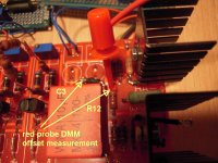
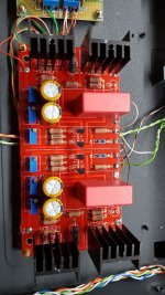
Offset measurement at BA-3FE
Hello BA-3-builders,
the following pics show, where I measure offset of the BA-3 frontend.
It doesn't matter if you put your red probe to the correct side of R12 or
of C3 - because they are directly connected by a trace on the pcb.
This PCB was used for a lot of testing - so it looks..... 🙄
The offset is fluctuating some mV around. This is a normal behaviour of this circuit. If you bias higher - give the Mosfets time to warm up a little bit.
But then it will be pretty stable.
You should easily get below 10mV offset - below 1mV is really good.
Greets
Dirk 😀
Attachments

Really nice. Thanks! That is how I did it in the end. I have been thinking, and maybe my positioning of the R12 probe was unstable, or touched the MOSFET heatsink (though not conductive). Another fluke in the house now, so will check tomorrow.
Btw: you say higher bias means less and more stable offset. How high can you bias with those heatsinks? I have the same, wanna go to 1,25 volts, but uncertain if I should start with that or standard 1v.
Btw: did it help in any aignificant way tieing the JFETs together like that?
Regards,
Andreas
Btw: you say higher bias means less and more stable offset. How high can you bias with those heatsinks? I have the same, wanna go to 1,25 volts, but uncertain if I should start with that or standard 1v.
Btw: did it help in any aignificant way tieing the JFETs together like that?
Regards,
Andreas
Last edited:
to andynor #453
Hello Andy,
as higher your bias as higher is the sensitivity of the offset (my experience).
I saw this behaviour especially at a bias voltage over R10 and R11 between
900mV and 1V.
Only minimal adjustments at P1 or P2 made a huge difference at the offset
( in the range of 900mV to 1v over R10/R11).
I got close to 950mV over R10/R11 but never biased higher. Heatsink temperature was not the problem. It was more runaway of my measured values.
The JFets are tied together with heatshrink to get a better thermal coupling
(between the N-channel- and P-channel- JFet). It can help to stabilize. But it doesn't make a big difference to me. I have made one board without the thermal coupling/heatshrink and it behaves very similar.
It gets better if your case / toplid is closed and no wind/airblows influence
the active devices ( good thermal equilibrium in the case).
Cheers
Dirk
Thanks! Your advice is really appreciated. Good news btw, is that I have now permanently mounted the FE. Stable offset of 19-20mv, but this is without fine tuning of p1 and 2. equal bias though on both mosfets per side. I take it as good news. Also, I managed to finish one side of the amp, and bias up the output board. Nice temp too. Anyway, confirmed it worked, so now off to the next side. Hope to finish within a week, then over to biasing things taking good time.
I built 3rd BA3 preamp for a friend. But this one has strong white noise on one channel. Couldn't find any miswiring, voltage problem or component mismatch.
Biasing fine for both channel, offset is acceptable. But somehow one channel has strong hissing sound.
Used linear systems jfets and fairchild fets.
😕
Biasing fine for both channel, offset is acceptable. But somehow one channel has strong hissing sound.
Used linear systems jfets and fairchild fets.
😕
Attached.
I accidentally replied to amp thread. Sorry about that.
I accidentally replied to amp thread. Sorry about that.
Attachments
Last edited:
I am no expert. And today I destroyed a bias PCB due to loosening a solder joint. But I would start by reflowing all solder joints where the solder has not flowed completely through. Especially on your JFETs. Also, rinse the board thoroughly to remove all flux, on both sides. Thats my two cents, awaiting Zen Mod to enlighten us all.
Attached.
I accidentally replied to amp thread. Sorry about that.
is PSU common for both channels ?
I am no expert. And today I destroyed a bias PCB due to loosening a solder joint. But I would start by reflowing all solder joints where the solder has not flowed completely through. Especially on your JFETs. Also, rinse the board thoroughly to remove all flux, on both sides. Thats my two cents, awaiting Zen Mod to enlighten us all.
improvise, or buy another pcb ( set)
I would improvise - waste to change entire populated pcb just because of few pads
- Home
- Amplifiers
- Pass Labs
- BA-3 Amplifier illustrated build guide