What are you using for a soldering iron? Solder is very important, as is a proper iron. One that maintains heat constantly by ramping up power when tip wants to cool contacting the joint to be.
Hakko begins a little north of $100 new, there are some "clones" of older Hakko models much cheaper. This improved my soldering a lot. Perfect joints became much, much easier.
Russellc
Hakko begins a little north of $100 new, there are some "clones" of older Hakko models much cheaper. This improved my soldering a lot. Perfect joints became much, much easier.
Russellc
I have a Weller WE1010 soldering station. Cost enough for me to expect that is not the issue. All other joints are no problem. Those joints, hard as hell. I have to get it fixed by someone professional. Unnessescarily small, I would say.
What are you using for a soldering iron? Solder is very important, as is a proper iron. One that maintains heat constantly by ramping up power when tip wants to cool contacting the joint to be.
Hakko begins a little north of $100 new, there are some "clones" of older Hakko models much cheaper. This improved my soldering a lot. Perfect joints became much, much easier.
Russellc
It could of course be the soldering iron, but I rather think it has to do with my own soldering skills combined with the fact the soldering joint is too natrow to get my 0,7mm solder to melt.
I looked that Iron up, I think you are just fine there, solder and technique are very important as well. Practice makes perfect. Iron to both leg and pad...pad is important. Add solder once the pad will melt it, then it should flow over the joint just fine.
Russellc
Russellc
I think you are right on the mark. What I now dread is having to unsolder some of the FETs. I have an aquaintance that might be able to help, and maybe learn a few tricks on how to unmess the mess I make. I think the main problem on these exact joints, which are smaller then all the rest of the joints on the FE, is that I did not take enough care to have a clean tip before making the first connections. So some joints turned out cold, and that is the mess I need to undo. The joints are so small I struggle seeing then properly. So a new work lsmp and a magnifying lens might be appropriate as well. Supreme f*** up...
Last edited:
No problem....when you install the precious Jfets, whether Toshiba or LS, leave plenty of lead and the Jfet standing tall. This makes it easy to remove, (cut it off) then poke out the little wire while heating. with the extra leads left on Jfet from "tall"mounting you can reuse it with ease.
I don't think anyone mentioned this yet, but magnifying hobby thingies are great here, and not expensive. 25-30 bucks, various strength lens, and a LED to light you target up.
Russellc
I don't think anyone mentioned this yet, but magnifying hobby thingies are great here, and not expensive. 25-30 bucks, various strength lens, and a LED to light you target up.
Russellc
Thanks! I’ll leave this subject at that, I see I took it a bit out of topic. But to be clear: It is the 4 MOSFET solder pads I find smaller than the others. The rest of the board is fine, I managed to solder nicely and think all the joints are good enough. I’ll post a pic later... But the MOSFETS: 50 percent OK, the rest cold or otherwise failed joints. I did not manage to wet the pad sufficiently. Argh... I will definitely order a lens with LED. Maybe some real fat greasy flux too. Only have the liquid one. Anyways, I am kinda disapointed about the MOSFET soldering job i did, seeing as the rest of the board was successful. But only solution is to learn from my mistakes. I will do this. But one of the solder pads is a bit black, probably from the extra flux i used. If I manage to clean my own mess up, I know I’ll succeed. If not, worst case scenario is ordering an extra board or two. As I am the only one having this issue, I guess this really highlights the level of my amateurism.
Thanks guys, really!
Thanks guys, really!
Last edited:
order a lens with LED. Maybe some real fat greasy flux too. Only have the liquid one.
Lens is extremely helpful!.
Careful about the fat greasy flux though.
When I began my journey, I got myself some cardas flux, which is more like Kolofonium (stuff used with string instruments). Joints were good, but they got covered with an ugly smear of that residue, which was rather hard to remove. I don’t use flux anymore.
Agreed. From Andynor's earlier posts I got the distinct impression his solder is
not the easiest to work with.
not the easiest to work with.
It is not a silver alloy. It is 63/37. It is a really good solder. But it had very little flux. So it is a one chance solder. It does not easily reflow when reheated. But finally I now have bought some no clean liquid flux. This means i can add some mote flux if need be, and reflow. Main problem has been my technique, and this solder revealed it more than I had hoped. 😱
Last edited:
Just saying, try the recommended solders, fire metal not available, but plenty of others. Good solder isnt one chance and it flows well when reheated. forget the add on flux, not needed and just causes a mess.
Russellc
Russellc
So far so good.
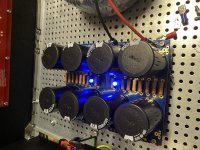
PSU finally up and running. 33,5 volts on the rails. Quite happy with the results, and nothing blew up despite no variac or light bulb test lead. Yes, I am taking chances, I know.
Notice I have split the rectifiers from the board. This choice was made in order to move the rectifiers and AC leads as far away as possible from the signal wires and gain stage. Another benefit is easy access to bias pots, as well as dissipation straight up through the top plate. Bias boards are planned on each side of the gain stage, to achieve ease of access.
The gain stage will be positioned above the PSU, and ensure only 5-7 cm of signal wire, as well as good physical distance from the noisy parts of the amp. I will use standoffs and a mounting plate from Modushop to achieve this positioning.
Attachments

Proper dressing of wires is good practice. For what it's worth, I can tell you this amp has NO propensity to hum at all. Mine is the quietest Amp I have ever had. You can listen at the driver and nothing. literally dead quiet. The only give away that it is on is the led glowing on.
Russellc
Russellc
Thansk, Russel! I teally appreciate you following my project and sharing you valuable experience with me and the community.
On another note, I have biased one channel of the FE now. Stable bias, and absolutely ZERO DC offset. Is this normal? I am not complaining, it is a very good thing. But since it is to be measured, and i do not get a reading basically, I have to ask =)
On another note, I have biased one channel of the FE now. Stable bias, and absolutely ZERO DC offset. Is this normal? I am not complaining, it is a very good thing. But since it is to be measured, and i do not get a reading basically, I have to ask =)
to andynor #435
Hello Andy,
if you bias your BA-3-FE up you should measure an offset at the output (during the biasing procedure).
-P3 is in mid position (don't dial there)
- adjust only one channel
You use two or three DMMs:
1st DMM measures the voltage over bias resistor R10 (in mV - up to 1V max.)
this voltage is adjusted by POT 2
2nd DMM measures the voltage over bias resistor R11 (in mV)
this voltage is adjusted by POT1
3rd DMM measures offset voltage (in mV) from output (before outputcap!) to ground
If you increase / dial up POT 1 then you will see an 'imbalance' of the voltages over the bias resistors R11 and R10 and as a result there will appear an offset
at the output.
I dial up POT 1 till I see an offset at the output of circa 50mV to 100mV.
Then I dial up POT2 till I get the offset at the output close to zero mV.
then same procedure again:
dial POT1 up till offset at output around 50 - 100mV
dial POT2 up till offset at output at ~ zero mV
As higher you get with the bias voltage (1V max.!) over R10/ R11 as more 'sensitive' the circuit will react on dialing at the POTs (my experience).
So, this is why I am confused, that you don't see/measure any offset???? 😕
Greets
Dirk 😉
Thanks a lot, Dirk! An explanation is in order. I initially just wanted to check if the circuit worked, IOW that verify that nothing blew up. When it did not blow up, I tried to see if I could get some voltage across R10 and 11. So I used only one DMM, moving it from R10 to 11 and back, and temporary psu connections. Moving to R12, i could only read 0mv. This might explain things. This was not a final bias procedure, just a test of blow-up risk before soldering any vables to the board.
I should add both transistors easily reeqced 0,8v and stabilized there, having the same temperature on their heatsinks approximately (to the touch).
Do you measure DC offset on R12 or R13? Or is R13 only for measuring IQ at this stage?
I have three DMMs and will connect them all next time I do some work.
Last edited:
to Andynor
Hello Andy,
I measure the offset with red probe between R12 and C3 (outputcap)
to ground (G on the board) - sure, black probe there.
All is looking good in your build! Take your time - especially during bias-procedure.
Success and good sound! - later....

Greets
Dirk
Hello Andy,
I measure the offset with red probe between R12 and C3 (outputcap)
to ground (G on the board) - sure, black probe there.
All is looking good in your build! Take your time - especially during bias-procedure.
Success and good sound! - later....
Greets
Dirk
Others please check / verify!
Andy, if it makes it easier for you to get the probes where they need to be... Here is what I did.
I was fortunate to have 3 DMMs, but only 2 sets of probes I could fix with hooks across R10 and R11.
So, I put the two fixed sets across R10 and R11 to measure bias. I installed a large cap in the "big" location for C3. Getting a probe to the "top" point on R12 (on the C3 side) was tight, and it was also too tight for me to get a probe to the "top" side of the big C3.
So, I used the "top" (-) point on the alternate, smaller C3 location (unpopulated) and GND to check my offset measurements.
The first page of the guide references measuring across R12. I believe that is incorrect (or maybe just not ideal), but I can't find my exact reference for when that was pointed out to me.
When you turn one pot (even a little bit) only, are you not seeing ANY change in offset?
tl;dr - The way Dirk describes is how I did mine, but I used slightly different points on the board that were easier for me to access reliably w/o risking shorting something with my probes.
Just sharing my experience for how I was able to get my probes in there and what measurement points I used. Please wait for someone with more knowledge to chime in. If I did it incorrectly and still got a functioning amp, it was blind luck. The amp sounds marvelous! 😀
Note - once you are ready for your full connections and build, recheck and rebias. At least with mine, it took QUITE some time to reach equilibrium once the full amp was built. With the top off, my input stage bias measurement stabilizes at ~0V9x. With the top on, it stabilizes at ~1V0x. As soon as I lift the lid, it drifts a bit. Try to be quick with your measurements. This is where having multiple DMMs really was a huge advantage for me.
Have fun with the build! 🙂
Thanks, very informative. I will do it again this afternoon.
Btw I put one connector to ground, and measured DC and was able to zero. BUT!
Funny thing is, i measured DC after my big cap. Is this normal? 0,9v, then I zeroed it by turning P2. But it was very sensitive, very small turns gave differences in DC readings after C3. Is my cap leaky? Maybe mpunted inversely (first pcb I ever soldered)? Or might it have to so with inputs not being shorted and outputs not connected?
Last edited:
- Home
- Amplifiers
- Pass Labs
- BA-3 Amplifier illustrated build guide