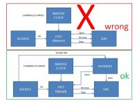
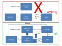
Right, but I would like to add that the crucial signal in digital to analog conversion is the DAC word clock, so you should slave the FIFO to the latch of the DAC.
In other word you need a very good master clock at lower frequency as possible (around 5MHz with appropriate dividers) to feed directly the DAC latch enable, then a FIFO slaved to the Master clock.
Attachments
I thought Ian's FIFO has the dividers on-board so the first option is actually a sub-set of the second one?
I thought Ian's FIFO has the dividers on-board so the first option is actually a sub-set of the second one?
No, the first option is how Ian's FIFO works, where the DAC is slaved to FIFO. In the second option the FIFO is slaved to DAC.
To implement the second option Ian should provide the sample rate to the dividers and should outputs data at high speed (Master clock) only when requested from the DAC by the latch signal. Finally he should stop the bit clock from the FIFO before the DAC is latching to avoid any interference between latch and bit clock.
Better if the communication between FIFO and DAC would optically isolated.
P.S.
I suggested 5/6 MHz clock because at these frequencies the crystals provide the best Q and the oscillators using these crystals have the best phase noise performance.
Last edited:
Ah, I see, that part about the DAC signaling the FIFO when it locks was not in the diagram.
I guess what you describe is not possible in my case where the ESS9038pro is in sync mode and thus DPLL is disabled and there is no locking to the clock, just assuming the master and data clock are in sync 🙂
I guess what you describe is not possible in my case where the ESS9038pro is in sync mode and thus DPLL is disabled and there is no locking to the clock, just assuming the master and data clock are in sync 🙂
Ah, I see, that part about the DAC signaling the FIFO when it locks was not in the diagram.
I guess what you describe is not possible in my case where the ESS9038pro is in sync mode and thus DPLL is disabled and there is no locking to the clock, just assuming the master and data clock are in sync 🙂
The Divider signaling the FIFO when it locks with the arrow labeled "Latch" from DIVIDERS to FIFO.
I don't know if you can implement this architecture with the Sabre. To do so you need the ESS9038pro to get async bit clock and latch, so the only master of the entire system is the latch from the dividers.
With opto-isolators.
Attachments
Last edited:
What is this "latch" thing with the DAC?
New terminology for me here.
The "latch" is the word select or the word clock.
I forgot an opto-isolator in the picture: between Source (or FIFO) and the divider. And to get the best isolation one should use Toslink devices.
The "latch" is the word select or the word clock.
'Word clock' for PCM is the same as LRCK, which is used to indicate the serial audio stream switching from Left channel bits to Right channel bits. The actual data bits are clocked into the dac by BCLK, the bit-clock.
Also, if serial audio is 16-bit, 24-bit, or 32-bit, causes BCLK to adjust in speed while LRCK stays the same for a given PCM sample rate.
IIRC, ESS says Sabre dacs I2S timing should ideally be synced with MCLK, the master clock, if using synchronous mode or master mode operation. To help facilitate being able to do that they have an option to export MCLK on a GPIO pin.
What is this "latch" thing with the DAC?
New terminology for me here.
A latch is basically a 1-bit memory. In a DAC (or any device that receives serial digital data) there is one for each data bit in a word, to hold the received bits until the whole word has been received. The clock controlling the latch determines at what point in time the particular bit is read.
Does it make any difference if there is a multi-channel usb-card, with or without (DIYINHK) galvanic isolation before McFifo? Why (not)?
Thanks to all who answered my questions regarding the latch and the merits of the FIFO solution. I've read them all. 🙂
Please find the attached FifoPi user's maunal (draft).
Ian
Ian, congrats!
Really well thought and written!
One question(referring page 6); does FifoPi only support DSD in the multiples of 44.1 kHz?
As one might have DSD in the multiples of 48 kHz as well; e.g. DSD 512 might mean both 44.1 x 512 = 22.579 Mhz and 48 x 512 = 24.576 Mhz, wondering whether FifoPi might support 48 kHz frequency family as well.
Thanks!
Thanks syracuze,
FifoPi supports DSD at multiples of both 44.1KHz and 48KHz. So, please no worry.
I didn't mention the 48KHz because SACD standard is mainly for 44.1 KHz group.
Regards,
Ian
FifoPi supports DSD at multiples of both 44.1KHz and 48KHz. So, please no worry.
I didn't mention the 48KHz because SACD standard is mainly for 44.1 KHz group.
Regards,
Ian
Thanks syracuze,
FifoPi supports DSD at multiples of both 44.1KHz and 48KHz. So, please no worry.
I didn't mention the 48KHz because SACD standard is mainly for 44.1 KHz group.
Regards,
Ian
Great! 🙂
Thanks!
Connect FifoPi to an I2S to HDMI output module
Hi Ian,
How do I connect the FifoPi to the AUDIO-GD DIY I2S to HDMI output module? The I2S to HDMI output module uses simple wires but the FifoPi uses U.FL connectors. Must I use some kind of adapter?
With regards, Bert.
Hi Ian,
How do I connect the FifoPi to the AUDIO-GD DIY I2S to HDMI output module? The I2S to HDMI output module uses simple wires but the FifoPi uses U.FL connectors. Must I use some kind of adapter?
An externally hosted image should be here but it was not working when we last tested it.
With regards, Bert.
@big bird
You can connect to the HDMI board through the isolated GPIO port on top of FifoPi.
FifoPi has three groups of output:
1. Isolated output in u.fl
2. Isolated output on GPIO
3. non-isolated output on additional GPIO.
So there will be no any problem.
Regards,
Ian
You can connect to the HDMI board through the isolated GPIO port on top of FifoPi.
FifoPi has three groups of output:
1. Isolated output in u.fl
2. Isolated output on GPIO
3. non-isolated output on additional GPIO.
So there will be no any problem.
Regards,
Ian
@big bird
BTW, I designed this I2S/DSD to HDMI transformer/receiver HATs, it can be plugged directly on top of the FifpPi. But the only problems is that I'm afraid they can not catch up with this GB. Hopefully I can make them available in a couple of months.
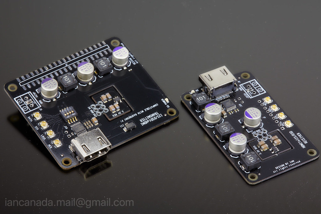
HDMI_I2S_DSD_KIT by Ian, on Flickr
Regards,
Ian
BTW, I designed this I2S/DSD to HDMI transformer/receiver HATs, it can be plugged directly on top of the FifpPi. But the only problems is that I'm afraid they can not catch up with this GB. Hopefully I can make them available in a couple of months.
HDMI_I2S_DSD_KIT by Ian, on Flickr
Regards,
Ian
Output voltage
Hi Ian
Which is the output voltage on I2S signals ? 5v ? 3.3v?
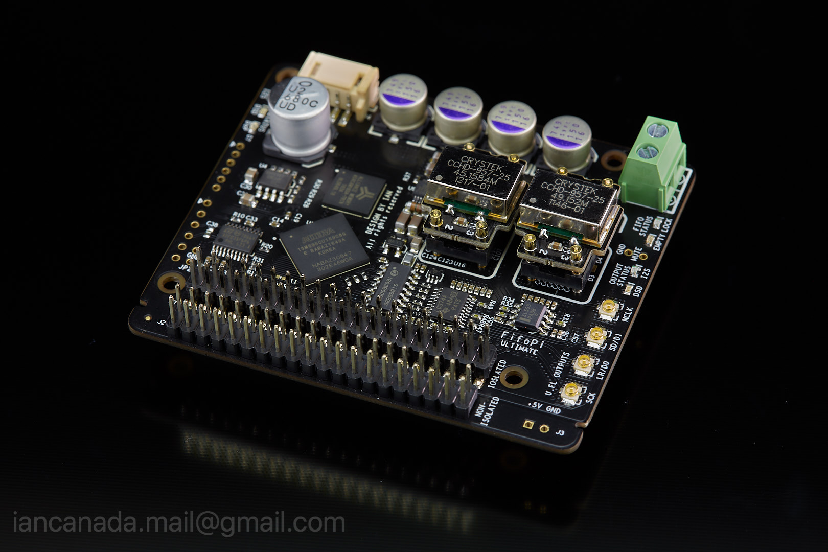
To achieve higher performance and better sound quality, I finally decided to design my own FIFO for raspberry Pi based on my third generation FIFO technology.
I'd like FifoPi to have the following features and specifications:
1. Up to 768KHz full range I2S support;
2. DSD64,128,256,512,1024;
3. built-in 768KHz DoP decoder to enable RaspberryPi native DSD play back up to DSD256;
4. Isolator board will be included;
5. Clock board (isolated) will also be integrated, works with interchangeable XOs through standard sockets or adapters;
6. Supports full rang of XO frequencies from 11.2894 to 98.3040MHz;
7. Has two DC inputs for both isolated clean power and RaspberryPi power;
8. Has an additional non-isolated GPIO connector to make DAC controller working in isolated mode;
9. Works with good 5V linear power through on-board low noise LDO or pure direct 3.3V power from ulatr-capacitor or LifePO4 battery power supply;
10 Works with all RPi DAC HAT and external high-end DAC at synchronized master clock mode to remove jitter;
11. Optional external display panel with adjustable delay time;
12. DIY friendly with options and flexibility.
FifoPi_1 by Ian, on Flickr
Ian
Hi Ian
Which is the output voltage on I2S signals ? 5v ? 3.3v?
- Home
- Source & Line
- Digital Line Level
- Asynchronous I2S FIFO project, an ultimate weapon to fight the jitter