It seems an odd design for the receptacle if that is all that note is about ... presumably it would become more of an issue with some insert/remove cycles on the connector leading to wear on that area below the receptacle.
Shorting is definitely a concern but I also recall being told something about rf something something considerations something.
Although that could just be my bad memory + talking to a certain square peg =P
Although that could just be my bad memory + talking to a certain square peg =P
Solder resist should never be used as a barrier against shorts, a sinilar problem exists with these type of connectors:
http://www.hirose.co.jp/cataloge_hp/e53700036.pdf
I always use a keep out area under the connector again to avoid shorts!
Just recently used these connectors with a cc1000 transmitter, ground plane under connector on an inner layer. This is just basic LPD433 stuff though.
If you are putting antennas on board the story is different, and different frequency RF will have its own problems and layout requirements. The main thing with these connectors for full RF is to keep the trace to the connector from the transmitter/Reciever at 50 ohms, on a two layer board this is a quite a wide trace.
Checked another board with mobile connectivity, again ground plane complete under the rf connector.
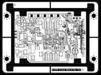
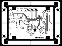
Revised Si570 based clock board PCB V2.0
Hi guys, good eye! PCB revised with route keepout. Please let me know for any suggestion. Thank you.
Ian
Hi Ian,
1. The hirose datasheet suggests removing ground plane from beneath the signal portion of the u.fl receptacle (see attached extract from hirose datasheet), it looks like your boards have the gnd continuing through this area? Is this a concern? I am far from knowledgable on these things just asking a honest question here.
The signalpart of the connector goes underneaath through that areato the central pin of the actualconnector, if the solder resist is a bit flakey it can short out. I would reccomend adding a keep out area to the actual footprint if your CAD package allows it, as it is one of those things you'll forget with this device otherwise, next time you use it! I know I have done in the past
Hi guys, good eye! PCB revised with route keepout. Please let me know for any suggestion. Thank you.
Ian
Attachments
Hi Ian,
The Si570 board progress looks very promising indeed! I have two questions though and I'm not sure if either or both have been covered previously.
2. Is it possible with the Si570 that the output stream may select a different *MCLK based on the input Fs?
Yes, it is. By taking the advantage of Si570, this board was specially designed with capability of output different MCLK frequency for a patiqular input Fs.
I have a DAC (ES9023) that I would like to use Fs*512 for Fs<=96kHz and Fs*256 for Fs>96kHz. Is this a possible configuration option via serial port? I will have either a microcontroller or an arm based linux board in the DAC enclosure so will be able to leave either of those permanently connected to the FIFO kit for 3rd party control if necessary.
That would be another back door 🙂. It will make things even more interesting.
Ian
Thanks Ian,
Now I am really looking forward to reading about your results of the next batch of prototypes!
Chris
Now I am really looking forward to reading about your results of the next batch of prototypes!
Chris
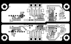
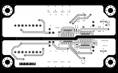
PCB layout of the FIFO digital isolator board
Except the isolators for bridging the FIFO and clock board, I placed a universal isolator at the empty space for some potential applications. That isolator chip could be IL715/IL716/IL717, or alternatives from Silicon Labs Si8440BB/Si8441BB/Si8442BB. The PUS could be independent from FIFO and clock on both sides by jumper settings.
It would be an interesting adapter. I might try to supply some free bare PCBs for evaluation after I get themJ.
Ian
Attachments
Nice. For this application, the Silabs devices are best choice because of their much lower cost.
excellent ian, do you think it will handle DSD? just thinking I might like to try one with the amanero Combo384 board
I would be interested in trying one out. Not that I care if free or at cost, but because I would like to play with the isolator🙂It would be an interesting adapter. I might try to supply some free bare PCBs for evaluation after I get themJ.
Ian
BTW is there an ETA for the Si570 clock board?
Cheers,
Nic
Another digital isolator for you would be the ADuM1400/1401 or 1402. You can find these here: Optocoupler Alternative | Analog Devices
Let me know what you think.
Let me know what you think.
hmmmm anyone got an IP on the above?
i'm going to assume you work at ADI, this is a non-commercial area
i'm going to assume you work at ADI, this is a non-commercial area
excellent ian, do you think it will handle DSD? just thinking I might like to try one with the amanero Combo384 board
I would be interested in trying one out. Not that I care if free or at cost, but because I would like to play with the isolator🙂
BTW is there an ETA for the Si570 clock board?
Cheers,
Nic
Ditto on trying one out Ian - Just say the word.
Nice! I would also be interested in trying one out so +1 for group buy.
Thanks guys for offering the try out. Will reserve one of the prototype PCB for each of you. Schematics will be provided then.
If it is possible, send me an email with your shipping address in order to post the PCB to you when I get them.
I may have 10 PCBs for free evaluation.
Have a nice weekend.
Ian
Nice. For this application, the Silabs devices are best choice because of their much lower cost.
I designed isolator footprints for both NVE and SiLabs. You can use either of them on each position. Kind of backdoor again 🙂.
They come from different technologies. NVE has chip transformers, while SiLabs is based on CMOS capacitors. For FIFO application, only isolation performance will be important. Of course SiLabs is less expensive (at least from digikey 🙂 ).
Nice weekend.
Ian
Last edited:
Another digital isolator for you would be the ADuM1400/1401 or 1402. You can find these here: Optocoupler Alternative | Analog Devices
Let me know what you think.
Fortunately isolators from ADI have compatible pins and footprint, I think they could be use also on this PCB.
Ian
I suppose if the result is positive, everyone with a FIFO board would want one and you'll manufacture them in quantities...
I suppose if the result is positive, everyone with a FIFO board would want one and you'll manufacture them in quantities...
Thanks. I think supplying PCB would be better 🙂, it's not that diffcult to solder this board.
To isolating the DAC from front end ground is a good idea. Many high speed ADC or DAC did this way.
Nice weekend.
Ian
- Home
- Source & Line
- Digital Line Level
- Asynchronous I2S FIFO project, an ultimate weapon to fight the jitter