Ricardo, congratulations for finishing your amplifier.
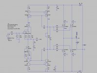
One thing that you can improve, is the fact that as you use the power supply far way from the amplifier board, you have to put reservoir capacitors (10000uf will be good) near the amplifier board to prevent the rectified class B currents from circulating in such a big loop, this capacitors will make this nasty currents circulate in a tight loop near the amplifier, keep the plus, minus and ground wires together also helps to prevent this currents from radiate.
One thing that is very important and I dont see it in the photo you take is the safety ground. That is very important , as a faulty transformer can make the amplifier case connected to the HV line , and that can be deadly.
Thank you for your input Sergio
My PSU case and the TX are connected to safety GND and I will take care of the amp's case as well.
As for the big caps near the OPS I really thought about that but did not have any in my stock at the time of build..... will do and report latter.
Worked and tweaked the design... seems like a strong concept.
I changed the cascode as it disrupted The current Circle.
That looks good to me, maybe I would replace R7 with a zener, and probably I would be using a vbe multiplier, but I would have to measure/simulate if this would change anything.
Yes, or it can be use a depletion mosfet like this.
This is super simple, it would be interesting to hear this one.

Yes duals will be good, to minimize thermal drift.
The mirror out TO126 must go on a heat-sink as it dissipates more than 1/2W.
The mirror out TO126 must go on a heat-sink as it dissipates more than 1/2W.
you can just select your own components, for the mirrors you can glue the transistors face to face to improve the tracking.
Member
Joined 2009
Paid Member
Can we focus on non SMD parts ?
I am not really at ease with those.... please
Just in case you were thinking about it in the future - just restrict yourself to using SMD for 2-terminal parts, namely resistors and diodes. Then use through-hole for everything else. Those 1206 resistors are not at all hard to deal with and once you have used them you might surprise yourself that you don't want to go back to using throuh hole resistors again. It makes for short path lengths, flexible pcb layout, less solder and no leads to clip.
just a normal High IDSS Jfet, good for CCS, just be aware the jfets are not very uniform, so JFETS CCS's alway needs trimming to reach the right current. here something like 6 mA is suitable.
http://search.alkon.net/cgi-bin/pdf.pl?pdfname=04368.pdf
http://www.onsemi.com/pub_link/Collateral/MMBF4391LT1-D.PDF
http://search.alkon.net/cgi-bin/pdf.pl?pdfname=04368.pdf
http://www.onsemi.com/pub_link/Collateral/MMBF4391LT1-D.PDF
Last edited:
The top transistors do not handle a lot of power or voltage, so a small low cob high HFE NPN-PNP macth will be the best. This is the reason for the suggested double
Going back to my actual amp, I would now like to try an emitter follower inside the miller loop.
Simulation seems ok but I would really appreciate some input regarding the schematic modifications and choice of values.
In order to lower input transistor current to the initial values I increased R3 from 680 to 1k1.
Can I use 2SA970 for the follower ? and what about it's emitter resistor... is 680 ok ?
Attachments
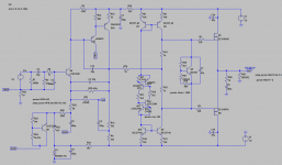
Going back to my actual amp, I would now like to try an emitter follower inside the miller loop.
Simulation seems ok but I would really appreciate some input regarding the schematic modifications and choice of values.
In order to lower input transistor current to the initial values I increased R3 from 680 to 1k1.
Can I use 2SA970 for the follower ? and what about it's emitter resistor... is 680 ok ?
My first choice would be 6mA = 200mW = 100/120 Ohm? I am thinking that 1mA is a bit to low. And: you must start using a Tian probe 🙂
Member
Joined 2009
Paid Member
Going back to my actual amp, I would now like to try an emitter follower inside the miller loop.
Simulation seems ok but I would really appreciate some input regarding the schematic modifications and choice of values.
In order to lower input transistor current to the initial values I increased R3 from 680 to 1k1.
Can I use 2SA970 for the follower ? and what about it's emitter resistor... is 680 ok ?
I wasn't able to run the attached file because it references external device models - you can embed the device models into the file (this is my usual practice so that the file can be run as-is). Anyhow, I remember running simulations with a few different values for TGM8 front-end and was happy with a little less current through the devices than seems popular. It's possible that I should have designed for more current but I have been pleased with the results. This may be an opportunity for you to advance the art, consider some more optimal operating points - try varying the values of the resistors and look at the FFT, open-loop-gain etc.
To simulate the open loop gain I resort to the simple approach of inserting an a.c. voltage source into the feedback loop and then plotting the ratio of the voltage on one side of it with respect to the other side as a function of frequency - you are effectively injecting a signal into the feedback loop and measuring the gain and phase. Somewhere around there there's a good link to see how it's done but I can't remember where it is - there may actually be an example file in the LTSpice examples folder. Edit: try here: http://www.linear.com/solutions/4449
Bear in mind that it's not quite as simple as it looks - the extra device is not just an emitter follower in the 'beta enhanced VAS' topology as D. Self calls it. The emitter follower is also used to directly bootstrap the collector load of the input transistor. Therefore, there is an interplay between the resistor values.
Last edited:
- Home
- Amplifiers
- Solid State
- Assemblage Power Amp