In summer 2010 in Moscow was +37C whole august 🙂 And seriously, it may be +35C around, if the amplifier placed in not good ventilated space, such as a shelf or a niche.Is the room temperature 35C in Russia?🙂
Thank you all for advices!
Sorry, Mr. Pass I did not express myself clearly, I was only a moment irritated that the
R5/R6 position was different in the upper and lower gate bias network of the CX1 PSU.
Once in the positive branch and once in the negativ branch....
Then I decided that you are right and that the position of this resistor is possible in both ways......
🙂
R5/R6 position was different in the upper and lower gate bias network of the CX1 PSU.
Once in the positive branch and once in the negativ branch....
Then I decided that you are right and that the position of this resistor is possible in both ways......
🙂
they're exactly where needed to be
one side need to be firm (ref. PSU rail) , while other side need to be adjustable
in other words - where 1mF is , that's firm side , where 3K3 is , that's adjustable side
remember this one ?
one side need to be firm (ref. PSU rail) , while other side need to be adjustable
in other words - where 1mF is , that's firm side , where 3K3 is , that's adjustable side
remember this one ?

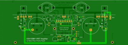
Here is a first proposal. The board measures 240mm*107mm. It bears all regulators an the input buffer. The jumpers J1 and J2 allow unbuffered balanced or buffered unbalanced mode.
Suggestions on improvements are welcome.
If there is likely to be a group buy for these boards I'd like a pair.
Thanks
Marra
If there is likely to be a group buy for these boards I'd like a pair.
Thanks
Marra
Terrific looking board, permaneder. I'd also like a pair when they become available. Thanks for the work on this - Pat
Here is a first proposal. The board measures 240mm*107mm. It bears all regulators an the input buffer. The jumpers J1 and J2 allow unbuffered balanced or buffered unbalanced mode.
Suggestions on improvements are welcome.
Hi Permaneder
I have send You PM about PCB's.Thanks
Maybe You can make new thread in group buys section ?
Greetings

Last edited:
with those minimal parts you still need a pricely PCB?.just add it up to the heatsinks. Well it might be good for a cosmetic look....if there's money why not...
Hm, I think it is fine for me to have all these regulations and gate bias circuits in one place...
And very short distances....!
And I am normally a PTP fan.....BUT....
I do not know why..... Building a complicated amp circuit is pleasure for me even in PTP, but an easy Amp circuit and four PSU circuits is so dull....
I know it is not logical, but my feeling....
🙂
And very short distances....!
And I am normally a PTP fan.....BUT....
I do not know why..... Building a complicated amp circuit is pleasure for me even in PTP, but an easy Amp circuit and four PSU circuits is so dull....
I know it is not logical, but my feeling....
🙂
Tastes are tastes.
I like the board. If we realize a preamp gain for it. All together in a board.
I like the board. If we realize a preamp gain for it. All together in a board.
Only difference I see, is that you have a big 22000uF cap after the regulator. At first sight I thought is was before the regulator as part of the PSU.
It helps to improve the supply.
Here is a first proposal. The board measures 240mm*107mm. It bears all regulators an the input buffer. The jumpers J1 and J2 allow unbuffered balanced or buffered unbalanced mode.
Suggestions on improvements are welcome.
Hi Permaneder
Can this PCB have supplementary holes for fixing with screws on the chassis and L profile ?
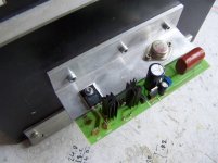
This circuit have much weight with Jensen and 22000 uF capacitors on.
I don't see any in your final pcb CCS L'amp version and Vfet...
Thanks for Your great work !
Greetings 🙂
Attachments
Last edited:
SONY VFET
Yes. Not really necessay yet. The 2.2mm thick board is stiff enough.
Hi Permaneder
Can this PCB have supplementary holes for fixing with screws on the chassis and L profile ?
This circuit have much weight with Jensen and 22000 uF capacitors on.
I don't see any in your final pcb CCS L'amp version and Vfet...
Thanks for Your great work !
Greetings 🙂
Yes. Not really necessay yet. The 2.2mm thick board is stiff enough.
Attachments
 Would have loved some small surface mounts though!
 of course I am in too for two pairs…..!
😀
The actual price for a set (2 boards) will be around EUR 30 + shipping cost.
Last edited:
- Status
- Not open for further replies.
- Home
- Amplifiers
- Pass Labs
- Article - Sony VFETs part 1