- Finding and asking Mr. X to provide the pcb files
Mr. X is diyAudio member s3tup.
diyAudio - View Profile: s3tup
Small Mistakes in Mr. X's schematics
Hi all,
Unfortunately there are some mistakes in the Mr. s3tup schematics.
But you'll detect them.
That is not the problem. The design is still sound.
However, this is not a complete dac design.
It is a:
- TDA1541x -based pcb
- peripheral circuits
- output stage (which I do not recmmend).
I could not find any info on his 'MCK' design and clk-distribution.
- For Digital Input Reciever + MCK Recovery, I highly recmmend the
Tentlabs Dac Implementation. (yes, yes I know you refuse to use it).
However, it is highly unlikely for diy:ers to do any better.
-if not, stay with the CS8412 or CS8414, do not go with the DIR 9xxx or WM88xx.
-
Last edited:
Hey Alexiss, thanks for catching the errors, good eye! 
It's not that I refuse the TentLabs implementation but rather I am looking for a design that's almost-good-to-go and I'm unsure how to competently interface a TDA1541 board with the completed TentLabs PCB (although that's starting to look like a good option ...)
I understand now that you were suggesting to use the Tentlabs info to design a Tentlabs front end with a 1541 DAC but that's beyond my skills and time and probably beyond the directionless nature of this thread.
I'm also looking for a USB front end, $100 for just the PCB is a bit steep, the Tentlabs info is old and doesn't use SM tech and it may be difficult to find the parts ...
That said however ... 😉
Tentlabs PCB as DAC platform ...
As Alexiss has perceptively suggested, the Tentlabs info and PCB is very sound and the older DIP technology (as expertly implemented) may be a good fit for DIY! 😀
Here's the start page for Tentlabs DIY:
Welcome to the Audio DAC page
The second link contains most of the great info:
Technical Overview
And here are the schematics and PCB layout info (but not the digital board):
Schematics
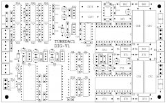
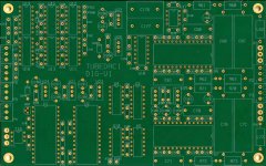
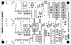
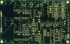
They say on the "Yes, I Want to Build a DAC" page that:
The information regarding the 3rd (digital) PCB is not given away. Few reasons are:
It is a 4-layer board, the result of an enormous amount of work.
A 4-layer board can only be made by professionals.
Ordering only one piece for your own will be very expensive.
But since this is an older design perhaps after asking we could get the manufacturing files and have our own boards made (might be much cheaper now than in 2001)
I've only corresponded with Guido a couple of times, hey Alexiss are you chummy with him or any of the other contributors? (Marc, Korneel, Jos or Guido) from: Project Description
Is anyone friendly with any of them and could thus act as our best ambassador?
As Alexiss has perceptively suggested, the Tentlabs info and PCB is very sound and the older DIP technology (as expertly implemented) may be a good fit for DIY! 😀
Here's the start page for Tentlabs DIY:
Welcome to the Audio DAC page
The second link contains most of the great info:
Technical Overview
And here are the schematics and PCB layout info (but not the digital board):
Schematics


They say on the "Yes, I Want to Build a DAC" page that:
The information regarding the 3rd (digital) PCB is not given away. Few reasons are:
It is a 4-layer board, the result of an enormous amount of work.
A 4-layer board can only be made by professionals.
Ordering only one piece for your own will be very expensive.
But since this is an older design perhaps after asking we could get the manufacturing files and have our own boards made (might be much cheaper now than in 2001)
I've only corresponded with Guido a couple of times, hey Alexiss are you chummy with him or any of the other contributors? (Marc, Korneel, Jos or Guido) from: Project Description
Is anyone friendly with any of them and could thus act as our best ambassador?
Last edited:
When it comes to Digital Input Section,
I have nothing right now. That is:
a complete design: schematics + description + pcb files that guys can use here.
I have seen many clever solutions here at diyaudio, but they are all (the ones that I have seen) improperly
designed or implemented (Please forgive me, I mean no disrespect, they just are - I am sorry).
This will in turn lead to higher and... let's say 'less suitable' jitter
characteristics than the lowly CS84xx.
I would therefore recommend staying with the CS84xx, as it would
be much more straight-forward to get 'fairly' close to the 200ps jitter specs
of the device.
As it turns out, CS8412 + Peripheral Circuitry by Mr. X + TDA1541
can perform very well indeed.
-
Last edited:
...Hey Alexiss are you chummy with him or any of the other contributors? (Marc, Korneel, Jos or Guido) from: Project Description
Unfortunately, I do not know any of them.
Is anyone friendly with any of them and could thus act as our best ambassador?
- Not a bad idea.
- However, I don't think they will,
- I am not sure if it will even be helpful.
The design of their Input Reciever is technologically sound, well documented, and it
will perform in a civilized manner (low jitter)
If anyone here think they can do better, then they are either:
- VERY experienced and VERY well-equipped Electronics Professionals
- or complete rookies (as they do not understand what they are talking about).
-
Hi Audiolapdance,
Alexiis said he doesn't know him in a post above.
Marce fellow, expert in RF in his job, said in another thread ('wire/cable for I2S thread if my memory is good") than the cost of small quantity of units falls a lot those days !
I saw expert inputs like Marce fellow's very impressive : he could may help us but he is very busy in him job as he is a professional designer in High RF electronic ! If he read us, just hints could help us if you can...Marce !
It can be an emergency exit than adapt Tents pcb but impossible without the files and a good drawner and/or designer. There are some here, if they want participate they are welcome !
Sure the Vanofonk's PCB improvement sould be more easier . What do you think to maybe create a thread with the permission of Vanofonk to look for enthusiast in RF here ? Oliver (redBaron) if he want could be a leads, I'm sure he read us.
A goal could be: he helps us because he can draw and he promiss to sell the pcbs cheap enough just for DIY and non commercial mass market with a contribution to DIYAUDIO like he does already with REDBARON V5, he keeps an amount for the effort & logistic ; win-win exchange if Vanofonk agree ? He deals already with contigous ground plain !
Audiolapdance do succeed open the file with a free version of Eagle ? Difficult ?
I try to have ideas as I have not a clue (ni marteau) about technics ! I asked elsewhere about TL431 regs (include in the Vanofonk's pcb) in powersupply section.
Last edited:
...I asked elsewhere about TL431 regs (include in the Vanofonk's pcb) in powersupply section.
Yes, I received it, and I posted my reply:
http://www.diyaudio.com/forums/digi...any-good-tda1541a-dac-kit-80.html#post3888626
Hi all,
Yep, my 1541 project was abandoned one, due to different things i've stuck with:
1. To evaluate the design you have to listen to it. My amplifier is on the worse side, so i began to build a new one, here.
2. To make this board work, and be worth of investement, you need
- A good low phase-noise clock. To make it, you have to measure it, understand it, etc. Lots of RF + low 1/f noise things in single design, which takes a while to figure it out.
- A digital interface board. Including digital filter, and some sort of suncronizing music source with the DAC clock. I began to draw it here. Stuck with the demanding design, as
- I tried to make it fitting any old DACs
- I tried to make it possible to operate it without compatible back-syncing sources as regular SPDIF. That requires low-noise path of recovered SPDIF clock and everything.
Thus, the PCB should be low-noise, high-speed, low EMI, and have a plenty of logic elements and customization. Yep, there is CPLD too, which you have to program.
To ummarize - this PCB should be absolutely analog, RF, digitally allow 0Hz to 10s of MHz, with BW of 0.5GHz, everything clean, matched AND low impedance. When i tried to route it, i've figured out i either have to cross traces with other traces, or go 4-layer. As i have to implement three dimensions of traces - power, signal and control, all over the PCB. Given we need to make as much of signal integrity as possible, we get 4layers quickly.
- Outut stages (I/V converters + filters) should be placed on the same PCB as DAC, as you don't want the return currents of DAC signal to flow all over the place. They come from PS rails and decoupling of I/V converter. Yet we'd like some degree of experimentation, thus removable PCBs.
As of sharing.
- I'm not interested in selling PCBs as they require debugging skills to be implemented. Thus support. Thus headache. They aren't ready for use anyway, as newer been fully powered on.
- No release of gerbers for this time. I don't want to spawn "group buys" of any sort, nor the "do it for me" 3rd party services.
- The design files are of Altium, a pricey piece of magic software. No value of DIY community as it is way too pricey.
So, to summarize, you get what you see - unfinished schematics, layout, and hopefully by the end of the following week - part values used in actual working implementation (i'm powering the thing on right now, with all the debugging involved). For your inspiration.
Please notice, this is my 2nd PCB in my lifetime, the transistor footprints are reversed, i've got some mistakes of power calcutations (but they seem to be OK). Since the "completion" of the board i've learnt quite a lot of current flows when i designed the power amplifier, and EMI/EMC stuff when i've tried to understand all sorts of it...
The PCB needs rework. Most of it is fine, yet all of the connectors should be placed on single side of the board, the 4-channel DFF should be replaced with tinylogic of some sort, larger DFF footprint on DEM-clocker, and i have no idea what else, yet several cycles of design reviews will prove i'm wrong.
The Digi-interface board might be obsolete, as i'm currently thinking about more sophisticated implementation, either around bad-*** FPGA or with fast MCU to do all the async stuff, lifting out all the "low-noise" thing out of the board into separate clock PCBs...
Or make it dirt-simple - 44.1k clock only, single DF, single back-synced SPDIF or USB.
2. To make this board work, and be worth of investement, you need
- A good low phase-noise clock. To make it, you have to measure it, understand it, etc. Lots of RF + low 1/f noise things in single design, which takes a while to figure it out.
- A digital interface board. Including digital filter, and some sort of suncronizing music source with the DAC clock. I began to draw it here. Stuck with the demanding design, as
- I tried to make it fitting any old DACs
- I tried to make it possible to operate it without compatible back-syncing sources as regular SPDIF. That requires low-noise path of recovered SPDIF clock and everything.
Thus, the PCB should be low-noise, high-speed, low EMI, and have a plenty of logic elements and customization. Yep, there is CPLD too, which you have to program.
To ummarize - this PCB should be absolutely analog, RF, digitally allow 0Hz to 10s of MHz, with BW of 0.5GHz, everything clean, matched AND low impedance. When i tried to route it, i've figured out i either have to cross traces with other traces, or go 4-layer. As i have to implement three dimensions of traces - power, signal and control, all over the PCB. Given we need to make as much of signal integrity as possible, we get 4layers quickly.
Once again: Hallelluyah.
As of sharing.
- I'm not interested in selling PCBs as they require debugging skills to be implemented. Thus support. Thus headache. They aren't ready for use anyway, as newer been fully powered on.
- No release of gerbers for this time. I don't want to spawn "group buys" of any sort, nor the "do it for me" 3rd party services.
- The design files are of Altium, a pricey piece of magic software. No value of DIY community as it is way too pricey.
Fully understandable, thanks for the heads-up.
Best Regards: Alexiss
-
Alexiss, thank you for your warm words and noticing my efforts 🙂
Yet we have to thank Mr. T., Nazar and many others who shared their knowledge here and all over the internet.
My pcb is just a mix of these, so my part in the design is quite tiny 🙂
Yet we have to thank Mr. T., Nazar and many others who shared their knowledge here and all over the internet.
My pcb is just a mix of these, so my part in the design is quite tiny 🙂
Hi, thank you to share your design, 🙂
Don't be so modest, your comprehension of digital is far better in relation to most of us. I aprreciated a lot your contributions and inputs in ECDESIGN's thread. You are welcome here if you want and have time enough. Maybe just some testimonies of what you listen to today (devices, DIY) could help us in our naive quest.
s3tup : There are some fellows like Andre mori who work about clock and seem agree to share. For the money if we have a team maybe we can organise a GB for money to test and some pcbs as i already wrote ! Maybe I'm naive, but from my seat the harder seems to make an aeropage of people who want to share. Audiolapdance had a good idea to beam the effort on a already existing concret pcb like the vanoFonk one. maybe I'm naive but with enough goodwilled people a lot of walls can be climbed....
@ Alexiss: yes I saw your answer, I'm looking for also others inputs: it's always about synergies: the more input, the more little contributions could help. I will spend time and continue personal effort to merge the inputs like Audiolapdance as my only useful contribution is time given and will to share and advance. thank you again for your inputs
Last edited:
This is a quote from post 605:
Quote:
I also have a lot of admiration to Thorsten and his work, based (also) on the sound quality of his products.
He was sharing his knowledge willingly and freely for decades, perhaps without the recognition he deserves.
I can assure you that a lot of individuals, including myself, admire his work and his kindness to share.
There are many like Mr Loesch and I salute them all.
@ Alexiss: yes I saw your answer, I'm looking for also others inputs: it's always about synergies: the more input, the more little contributions could help. I will spend time and continue personal effort to merge the inputs like Audiolapdance as my only useful contribution is time given and will to share and advance. thank you again for your inputs
- I think your design is very good.
- Not much more is necessary.
- As I said, it can be directly applied to TDA1541 ( +5, -5 , -15), with very good results.
-
s3tup,
Sorry, I didn't read your input at #810. Forgett my invitation above. Thank you for your shared testimonies and for sharing what you have done already.
@ Alexiis : some inputs of fellows in PS section to make it less noisy because the TL431 is a shunt reg: a little beat noisy. I understood maybe it's good enough for TDA1541 as its architecture is not CMOS...
regards
eldam
@ Alexiis :
...some inputs of fellows in PS section to make it less noisy because the TL431 is a shunt reg: a little beat noisy.
I understood maybe it's good enough for TDA1541 as its architecture is not CMOS...
- Who is claiming this?
- What is his background?
- How is he measuring?
- What is the definition of this 'noise'?
- What equipment is used to measure this 'noise'?
- What Measurement BW is used?
- What is the loading conditions?
- How is the circuit implemented? (schematics + pics of pcb)
This information is necessary before I can answer to your question.
Stating that something is 'noisy' in Circuit Design is the equivalent of going to a restaurant and saying 'food'.
-
Last edited:
There you are!  Thanks for coming!
Awesome, let us know how it turns out ...
Wait, ... so you're just ... teasing us!?! 😉
Surely we can come to some sort of compromise ... maybe a few of us in this thread could act as a "hassle buffer" and intercept any whining and unreasonable demands (like this very one 😱) before they bother you?
Or a few of us that have good measuring equipment (not me) could help you debug your design for your next revs ...
Some of us have been waiting so long for a reasonable and inexpensive 1541 PCB ... and yours is one of the best I've seen (very impressive for only your 2nd PCB!)
Don't make me beg ...
...
OK, I'm begging! But I'll respect your choices!
Cheers,
Jeff
 Thanks for coming!
...
So, to summarize, you get what you see - unfinished schematics, layout, and hopefully by the end of the following week - part values used in actual working implementation (i'm powering the thing on right now, with all the debugging involved). For your inspiration.
...
Awesome, let us know how it turns out ...
...
As of sharing.
- I'm not interested in selling PCBs as they require debugging skills to be implemented. Thus support. Thus headache. They aren't ready for use anyway, as newer been fully powered on.
- No release of gerbers for this time. I don't want to spawn "group buys" of any sort, nor the "do it for me" 3rd party services.
- The design files are of Altium, a pricey piece of magic software. No value of DIY community as it is way too pricey.
...
Wait, ... so you're just ... teasing us!?! 😉
Surely we can come to some sort of compromise ... maybe a few of us in this thread could act as a "hassle buffer" and intercept any whining and unreasonable demands (like this very one 😱) before they bother you?
Or a few of us that have good measuring equipment (not me) could help you debug your design for your next revs ...
Some of us have been waiting so long for a reasonable and inexpensive 1541 PCB ... and yours is one of the best I've seen (very impressive for only your 2nd PCB!)
Don't make me beg ...
...
OK, I'm begging!
 But I'll respect your choices!
Cheers,
Jeff
Last edited:
- Who is claiming this?
- What is his background?
- How is he measuring?
- What is his definition of this 'noise'?
- What equipment is used to measure this 'noise'?
- What Measurement BW is used?
- What is the loading conditions?
- How is the circuit implemented? (schematics + pics of pcb)
This information is necessary before I can answer.
-
Yikes ... I think it was T who mentioned the more unique 1541 architecture but I recall it was in relation to caps:
From: http://www.diyaudio.com/forums/digi...-any-good-tda1541a-dac-kit-4.html#post2854098
DEM Decoupling:
For the TDA1541 ONLY we can also use these SMD film cap's for the PSU rail decoupling. At the worst it will see around 6MHz clocks AND because the TDA1541 internally uses current steering (a non-standard ECL Logic essentially), so there is much less RF in the PSU Rails we need to decouple.
... and ...
Power Supplies:
Now power supplies. I would suggest using shunt regulators, however the important part is that shunt section is close to the TDA1541. Feed them from current sources, which can be remote and add a choke before the Shunt Reg.
There are many options, take your pick. I used TL431's on many of my DAC's and they work well, are compact and easily applied. But they can be bettered quite easily, but with more complexity. Similar tradeoff's apply to current sources.
And then from: http://www.diyaudio.com/forums/digi...any-good-tda1541a-dac-kit-13.html#post2862125
SMD film caps:
For the TDA1541 use the same SMD Film Cap's for both decoupling the DEM Pins (14pcs in total) and to decouple the supply pins (3).
Using 0.1uF Panasonic types in 1210 format (stand them on edge to fit) means they are effective to around 12MHz. As the TDA1541 is bipolar current steering based, it does behave rather different from modern CMOS chips in terms of PSU noise and has no real problems with this kind of decoupling, a CMOS chip on the other hand would be a disaster area decoupled like this.
Thank you Audiolapdance.
I believe Eldam is referring to the Noise in his suggested TL431 + Bipolar Transistor Series Regulator Design,
not Mr T.'s
description of DEM decoupling devices.
I think Eldam means how to reduce Noise in his regulator design.
-
I believe Eldam is referring to the Noise in his suggested TL431 + Bipolar Transistor Series Regulator Design,
not Mr T.'s
An externally hosted image should be here but it was not working when we last tested it.
description of DEM decoupling devices.
I think Eldam means how to reduce Noise in his regulator design.
-
Last edited:
- Status
- Not open for further replies.
- Home
- Source & Line
- Digital Line Level
- Any good TDA1541A DAC kit?