OK now I see that the decoupling caps are 200V ones I realise why they are so big. Looking forward to your comments on the sound and performance of this amp vs your other design.
Hi Quasi,
I got two questions:
1. Are you using 1/4W resistors?
2. Why did't you mount T4 under pcb into heatsink (or you will do this later)?
P.S. Nice PCB DIY-ing, I using the same spray (POSITIV20) but with neon UV lamp for aquariums (10W - 10min).
Regards...
Miodrag Pejin
I got two questions:
1. Are you using 1/4W resistors?
2. Why did't you mount T4 under pcb into heatsink (or you will do this later)?
P.S. Nice PCB DIY-ing, I using the same spray (POSITIV20) but with neon UV lamp for aquariums (10W - 10min).
Regards...
Miodrag Pejin
Hi Miodrag,
I use 0.5w metal film for all resistors except for the FET gate resistors (27R). These are 0.25w carbon.
T4 will be mounted when the heatsink is ready.
Hi Richie00boy, I'll post results as soon as I can. I still have a fair bit of work to do. As far a sound goes, the other one is going to be hard to beat. But we shall see what we shall see (hear).
Cheers
Hi Quasi, Amplifier Guru
Looks like every one of your cats will get a power amp for their birthday.
Very nice work. You're amassing quite a following of dedicated amplifier DIYers. It's also awesome that it does not require double-sided PCB.
What "other" one? I had understood that your other design was a bit noisy and you were designing this one as an improved version. I may be getting mixed up in all these different designs.
Andy
Looks like every one of your cats will get a power amp for their birthday.
Very nice work. You're amassing quite a following of dedicated amplifier DIYers. It's also awesome that it does not require double-sided PCB.
....As far a sound goes, the other one is going to be hard to beat.....
What "other" one? I had understood that your other design was a bit noisy and you were designing this one as an improved version. I may be getting mixed up in all these different designs.
Andy
Hi vectorplane
An earlier version of the amp in this thread is the noisy one. The other amp that will be hard to beat is this one; http://www.diyaudio.com/forums/attachment.php?s=&postid=818662&stamp=1137491636
Cheers & goodluck
An earlier version of the amp in this thread is the noisy one. The other amp that will be hard to beat is this one; http://www.diyaudio.com/forums/attachment.php?s=&postid=818662&stamp=1137491636
Cheers & goodluck
Thanks Quasi
I would like to produce an smd board layout for your amp. If anyone else is fond of smd components I can share this work when complete.
I'm just wondering... smd resistors are for the most part 1/8 or 1/10 watt I believe. Would any of the resistors in this shematic require a power greater than that (apart from the output source resistors of course)?
Andy
Hi Quasi,
you and a few others use low value bleed resistors.
Can you explain why?
I would tend towards higher values since I think their only benefit is to reduce the stored cap energy before prying fingers/tools go inside.
Maybe you know of others needs/advantages?
you and a few others use low value bleed resistors.
Can you explain why?
I would tend towards higher values since I think their only benefit is to reduce the stored cap energy before prying fingers/tools go inside.
Maybe you know of others needs/advantages?
A Small Advise to Brilliant Designer.....
Hi Quasi,
The Base + resistor of T8 must be connected to the collector of T7, in order to facilitate the full saturation of Negative rail side mosfets.... and increase the resistor value to about 1K instead of 22 ohms....
Secondly why you have limited the bandwidth of first differential with RC network comprising of C4 & R6...Since you already have VAS compensation caps on second differentials as well.....Too much compensation limits the slewrate...
Try to place the Bleeder resistor away from the Filter caps, or with the prolonged heating of resistor would eventually dries the electrolye in the cap...
regards,
K a n w a r
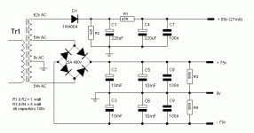
Hi AndrewT,
I choose a bleed resistor to discharge the capacitors within a reasonable time. I.e. for 75 volt rails a 6k8 resistor will discharge 20,000uF down to 10 volts in about 2 minutes. The resistor will dissipate 0.83 watts while the power supply is on. This to me is acceptable. Of course if the power supply is connected to the amp module the discharge time is a lot quicker.
I have read somewhere (this forum I think) that electrolytic capacitors like to discharge quickly, something about not hanging outside their ideal operating voltage for too long etc.....but I don't know about that.
Cheers
Re: A Small Advise to Brilliant Designer.....
Hi Kanwar,
Do you mean .....The Base + resistor of T7 must be connected to the collector of T8?
Cheers
Workhorse said:Hi Quasi,
The Base + resistor of T8 must be connected to the collector of T7, in order to facilitate the full saturation of Negative rail side mosfets.... and increase the resistor value to about 1K instead of 22 ohms....
K a n w a r
Hi Kanwar,
Do you mean .....The Base + resistor of T7 must be connected to the collector of T8?
Cheers
no....not at all...I mean to say connect the base of T8 through base resistor to the collector of T7
reminder:
The Base + resistor of T8 must be connected to the collector of T7, in order to facilitate the full saturation of Negative rail side mosfets.... and increase the resistor value to about 1K instead of 22 ohms....
Secondly why you have limited the bandwidth of first differential with RC network comprising of C4 & R6...Since you already have VAS compensation caps on second differentials as well.....Too much compensation limits the slewrate...
Try to place the Bleeder resistor away from the Filter caps, or with the prolonged heating of resistor would eventually dries the electrolye in the cap...
regards,
K a n w a r
!
Hi
How much power I will get with 3 pairs of IRFP250N and power suply +-75V DC?250RMS 8ohm?
Very nice amplifier!
Hi
How much power I will get with 3 pairs of IRFP250N and power suply +-75V DC?250RMS 8ohm?
Very nice amplifier!
Re: !
Is that you in the avatar....Viktor
viktor1986 said:Hi
How much power I will get with 3 pairs of IRFP250N and power suply +-75V DC?250RMS 8ohm?
Very nice amplifier!
Is that you in the avatar....Viktor
Hi Kanwar......
Regarding C5 & R6, I'm just too scared of oscillations. I might take them out during testing.
Regarding T7, can you please explaine more deeply. I've tried looking at the effect a large negative swing on the output will have, but to me this would just turn T7 on harder, reducing the voltage across it. There should still be plenty of drive from T6. Or have I missed something?
Cheers
Hello Viktor,
Lets try this for a typical setup;
75 volt rails at idle - 10% regulation at full power = 67.5 volts.
Say we lose 2 volts across FETs = 65.5.
so 65.5 x 0.707 = 46.3 volts RMS
equals 268 watts into 8 ohms resistive.
Cheers
Lets try this for a typical setup;
75 volt rails at idle - 10% regulation at full power = 67.5 volts.
Say we lose 2 volts across FETs = 65.5.
so 65.5 x 0.707 = 46.3 volts RMS
equals 268 watts into 8 ohms resistive.
Cheers
Workhorse said:no....not at all...I mean to say connect the base of T8 through base resistor to the collector of T7
reminder:
The Base + resistor of T8 must be connected to the collector of T7, in order to facilitate the full saturation of Negative rail side mosfets....
Sorry man I still don't get it. The negative rail FETs are driven by a constant current source T5 through T6 (half of the 2nd LTP). As T6's base swings negative T6 turns on harder swinging more current through R16. All T7 does is track the output swing setting its emitter 0.6 volts above that.
Can you describe your view in terms of voltages and current flows, so that I can follow you.
Cheers
Sorry Andy ....missed this.
R12 and R14 dissipate around 0.25 watts with 75 volt rails (85v driver rail). other resistors (except the 5 watt ones) should be ok.
Cheers
vectorplane said:Thanks Quasi
I would like to produce an smd board layout for your amp. If anyone else is fond of smd components I can share this work when complete.
I'm just wondering... smd resistors are for the most part 1/8 or 1/10 watt I believe. Would any of the resistors in this shematic require a power greater than that (apart from the output source resistors of course)?
Andy
R12 and R14 dissipate around 0.25 watts with 75 volt rails (85v driver rail). other resistors (except the 5 watt ones) should be ok.
Cheers
- Status
- Not open for further replies.
- Home
- Amplifiers
- Solid State
- Another quasi-complementary design