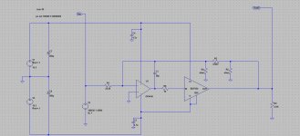
Sergey888 - ah, I understand now. 🙂 The equivalent conversion of the T to the delta is just to make it easier to see what the T network is really doing in the circuit.
I've attached a schematic below for anyone else out there who might be following along. Sure enough, as you say the R5 leg just loads the output of the buffer and R4 is between the inverting input and ground. That second leg to ground, R4, is an interesting thing. When I first designed the amp I actually had pads for a resistor to ground on that inverting input on purpose, to optionally implement this 14 year old post:
http://www.diyaudio.com/forums/solid-state/6558-opamp-inverting-input-sounds-better.html#post67880
from this thread
http://www.diyaudio.com/forums/solid-state/6558-opamp-inverting-input-sounds-better.html
Essentially Nelson is saying that the amp sounded better subjectively in some listening tests with 20dB of open loop gain thrown away. Your observation may be part of the reason. With less feedback certain distortion products might increase a bit. The net result might sound "better" in the sense that tube amps do at times with their inherent distortions, e.g. sgrossklass' post above.
You are right, with just the 33K there is no audible background noise just as it sits. Nothing that I could hear anyway with the volume and gain all the way up and sensitive cans. Alex has reported the same. The T network would be fixing a problem that doesn't exist, while creating other issues, at least in the case of this amp.
Thanks again for your insights here! 🙂
Attachments
Last edited:
Sergey888 - good point!
At 25C and 20KHz bandwidth the 24.9K input resistor should have somewhere around 2.9uVrms of Johnson noise. Gaining that input resistor noise up by the 1.33x stage voltage gain gives 2.9 * 1.33 = 3.89uVrms. The 33K feedback resistor should have 3.3uVrms.
I'm assuming that since the two noise sources are uncorrelated they would add in an RMS sum at the output for a total due to the resistors:
sqrt(3.89^2 + 3.3^2) = 5.1uVrms
The noise due to the OPA2140 should be
5.1nV/sqrt(Hz) * sqrt(20KHz * 1.57) = 0.90uVrms
multiplied by stage gain:
0.90uV * 1.33 = 1.2uVrms
if I have the math right. Looks like the resistors are noisier than the op-amp. 🙂
I'm not finding any noise graphs in the BUF634 datasheet The noise density graphs for the LME49600 in that datasheet show numbers about the same as the op-amp.
Last edited:
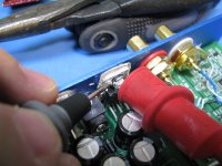
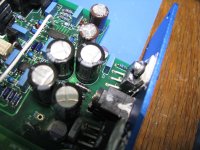
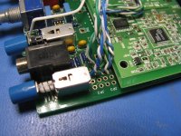
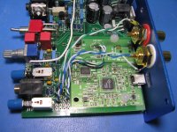
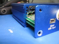
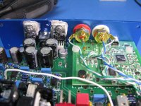
Wiring up the rear panel - part 1
A few posts ago I said that I would show wiring up the rear panel and mounting the two voltage regulators with the mounting hardware. Here it is in pictures.
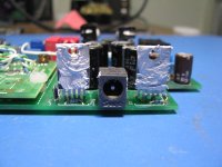
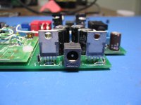
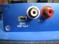
The RCA jacks are wired as a pass-through from the ODAC. The output of the ODAC goes to both the rear RCA jacks and to the input select switch on the front panel.
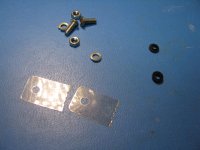
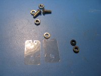
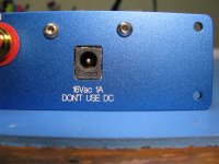
The vreg mounting bolts are 3mm x 8mm long, button head (M2 socket) stainless steel from Bolt Depot.
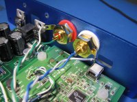
The meter is measuring for (lack of) continuity between the voltage regulator mounting bolt and the tab, once both of the insulating washers are in place and the nut tightened down. Just checking to see if the nylon washer was out of alignment and/or the mica washer was pierced.
A few posts ago I said that I would show wiring up the rear panel and mounting the two voltage regulators with the mounting hardware. Here it is in pictures.
The RCA jacks are wired as a pass-through from the ODAC. The output of the ODAC goes to both the rear RCA jacks and to the input select switch on the front panel.
The vreg mounting bolts are 3mm x 8mm long, button head (M2 socket) stainless steel from Bolt Depot.
The meter is measuring for (lack of) continuity between the voltage regulator mounting bolt and the tab, once both of the insulating washers are in place and the nut tightened down. Just checking to see if the nylon washer was out of alignment and/or the mica washer was pierced.
Attachments
-
 IMG_4078.JPG273.9 KB · Views: 95
 -
 IMG_4077.JPG297.9 KB · Views: 99
 -
 IMG_4075.JPG337.9 KB · Views: 108
 -
 IMG_4071.JPG236.2 KB · Views: 87
 -
 IMG_4070.JPG225.4 KB · Views: 87
 -
 IMG_4069.JPG283.5 KB · Views: 72
 -
 IMG_4068.JPG297.4 KB · Views: 199
 -
 IMG_4065.JPG342.1 KB · Views: 207
 -
 IMG_4064.JPG339.4 KB · Views: 208
 -
 IMG_4063.JPG371 KB · Views: 215
Last edited:
Wiring up the rear panel - part 2
I ran out of photo posting slots above -
The last photo is the final inspection. 😛
I ran out of photo posting slots above -
The last photo is the final inspection. 😛
Attachments

Last edited:
One of her cat toys is an old anti-stat wrist strap. Geeezzzz what a bad idea on my part. Didn't think that one through. Now she thinks any anti-stat wrist stap is a cat toy. I'll be soldering some delicate part and all of a sudden she sneaks up, jumps, and snags the wrist strap coils with the claws. 😱
Just to make sure... In case of the T net you'll get a higher output noise, since your input resistor in a noise model will be represented by R1||R4 (your last pic) and gained G=( R3/(R4||R1)) times. This is more than noise of R1 by (R3/R1) times (if R4 excluded). Also an opamp noise will be multiplied by (1 + R3/(R4||R1)) instead of just (1 + R3/R1).
Mistake in your Google doc Site
You have a folder labeled V3.61 1_5_2015, it should read v3.61 1_5_2016.😕
You need to fix the other references as well. Who hasn't typed 2015 when it
should be 2016. Great work.Our you going to do a Group buy and/or
kit buy? I sure hope so.😀
You have a folder labeled V3.61 1_5_2015, it should read v3.61 1_5_2016.😕
You need to fix the other references as well. Who hasn't typed 2015 when it
should be 2016.
Great work.Our you going to do a Group buy and/orkit buy? I sure hope so.😀
Thanks for letting me know about that folder name! Fixed now. 🙂
I have boards - I'll send you a PM.
I have boards - I'll send you a PM.
A new V3.61 BOM posted with a full set of Digikey part numbers
I've just posted an updated V3.61 BOM out at the project Google Drive link here. The major change is the addition of a full set of Digikey part numbers, similar to what I did with my ODA BOM a couple of weeks ago, in case someone wants to build the whole project from a Digikey order. I've gone through all the Mouser parts and updated prices, plus I've gone through the "notes" column and updated a few things.
A big "thanks" goes out to 4x4F150 for catching two errors in both the V3.6 and V3.61 BOMs! Both are corrected now. The RN50C resistors are all 1/20W, not 1/8W as was listed. The quantity of 100R resistors is 5 rather than 4 in the V3.61 BOM (the new clipping indicator sense line resistor). I hadn't formatted that cell correctly in the spreadsheet either which caused that extra resistor part number not to show.
I've added a new "readme" file on Google Drive with a reminder of the of the difference between V3.6 and V3.61. V3.6 is the only one I've made PC boards for. In V3.61 I made a very small change in the power supply voltage "set" resistors for the LT3080. Two 0.1% resistors & one 1% now rather than just two 1%. I also added a resistor to the clipping indicator sense line.
None of the changes make any difference at all to the performance of the amp. The "readme" has the details. Even though I haven't fabricated a V3.61 board I did generate the set of Gerber files for it and posted them here, hence the V3.61 BOM to match the V3.61 Gerbers.
If you are building a V3.6 board the V3.61 BOM is identical except that you don't have R40 or R41, and R7 is 1.5 meg 1% 1/8W rather than 1 meg 0.1% 1/4W. I haven't added a full Digikey column to the V3.6 BOM because it is a huge amount of work(!), so just use the V3.61 BOM for Digikey numbers noting those few changes in the "readme" file. If you only need the Mouser part numbers the you can continue to use the V3.6 BOM at the Google Drive project link.
Attachments
Last edited:
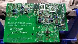
Started the build last week but ran into some issues with the resistors. Once again, agdr bailed me out with the correct parts. Thanks again agdr! I also managed to cut one of the small SMD caps in half with my flush cutters 😱 while trimming some leads from the through hole parts.
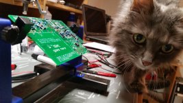
Everything went smooth this weekend and I have some pics of the progress. Below is a pic from end of step 2, and then end of step 3. I also included a picture of my four legged curious "helper" since it seems to be a theme with this thread 🙂
Hopefully will have this thing cranking out sound by the end of this weekend.
Attachments
4x4F150 - Looking good! Your SMD soldering is great. Clicking on the lower left of those pix will zoom them up.
Did you have any through-holes plug up with solder when soldering the 0603 1uF SMDs on the back? I've done those enough times now that I can usually make it through the whole bunch without plugging any nearby holes. One secret there is don't go back and touch up the original end of the cap after soldering the second end. Wait until the through hole part legs are in the nearby holes to touch up the SMD caps.
Good to see that your board is CAT scanned too! 😀
Did you have any through-holes plug up with solder when soldering the 0603 1uF SMDs on the back?
Nope, no problems with any of the holes. I read your warning about that before I started, so I was sure to watch out for it.
I do have a question though... I noticed that you recommended 22 gauge solid wire for the jumpers in the instructions, and I ran out of 22 gauge. I do have an endless supply of 24 gauge solid wire from all the cat 5e wire I have. Do you think 24 gauge will be thick enough for the jumpers, or should i just buy some more 22 gauge?
Do you think 24 gauge will be thick enough for the jumpers, or should i just buy some more 22 gauge?
Your cat5 24 gauge strands will be just fine. I wire stuff here with it all the time. 🙂 The maximum ampacity in closed spaces is still around 3 amps. I just specified 22 awg as being a little more mechanically robust during assembly. In my experience that is the big problem with 24 awg solid, you only get a handful of back and forth bends before it breaks. I just looked it up for fun. The breaking force for 24 awg is around 11 lbs. For 24 awg they list 18 lbs, the same as the 4" nylon tie-wraps.
Hey that is good to hear that you didn't have any trouble with the 0603 1uFs! Those are the one part of the project I had to think about for awhile because I knew they would be a bit of a soldering challenge. I used 0805 on the first version but they were too long. I plugged up the surrounding film cap through-holes about 1/2 the time. And just no extra board space to use through-hole 1uFs.
Last edited:
Good to know that the cat 5e cable will work... I have so much of it.
But my next question, why are the holes for IC5 and IC6 staggered? the chips I received have the leads in a straight line. I double checked the part numbers and they match the BOM. I assume I just need to bend the leads, but am hesitant to solder in because they do not mach the board. Thinking that the holes are staggered to make soldering easier and avoid bridges???
Also, you refer to 2 sets of heat sinks. One set is a temp set that is larger for use when testing the power supply while waiting on panel express to cut the back panel to specs. The other set is for permanent use on the output buffers. The BOM only lists one set of heat sinks, so I am a little confused. Where did I go wrong? (The BOM says that the heat sinks listed are for the buffers)
Sorry for the confusion.
Thinking that the holes are staggered to make soldering easier and avoid bridges???
Good questions! I will add some more info to the build instructions (and BOM) for both things.
That is exactly why the staggered holes, to make soldering less likely to bridge. A lot of TO-220's with more than 3 leads are already staggered, like the LT1963A, LT3015, and LT3080 voltage regulators I use. No need to pre-bend the leads either, other than separating out the 2 front ones a bit. I just stick the back 3 in their holes, then line up the front 2 and stick those in, then push the thing down. 🙂 Works great. One tip though - hopefully this is in the build instructions but I can't remember - pre-assemble the heat sink onto each BUF634 before soldering it in.
On those temporary rear heat sinks, you are right, I don't have those in the BOM and I should. When I put the BOM together I was just thinking rear panel for heatsinking. But in actual practice most folks wound up ordering their panels after the amp was together, so I started shipping any boards I sent out with those temporary heat sinks to use until a rear panel was in hand. Those have turned out to be pretty necessary and really should be in the BOM. The temp sinks for the rear panel are the ones with the longer fins - the BUF624 sinks are the shorter fins.
When I put the BOM together I was just thinking rear panel for heatsinking. But in actual practice most folks wound up ordering their panels after the amp was together, so I started shipping any boards I sent out with those temporary heat sinks to use until a rear panel was in hand.
Sounds good, just wanted to make sure. And FYI, I didn't get any heat sinks with the board but it doesn't matter because I found some left over ones from the ODA build. (I never used the temp heat sinks for the ODA) But that was my real cause for confusion... I only had one set of heat sinks for this board.
So, I used those left over heat sinks (they are bigger than the buffer ones) and tested my power supply last night. 15.30- VDC and 15.34+ VDC. Pretty accurate! Don't think I really need to correct 0.04 on the positive side, so I'm just going to leave as is (I also don't have the proper resistor to drop it down to match the negative, so that factored into the decision). That 1.5M resistor you sent was the reason I got so close to 15.3. Pretty sure I would have to drop the 30K to a 26K to make the positive match.
Going to be drilling the back panel tonight myself.... following adydula's lead here with sending the front to FPE and doing the back myself to save some $$$. Also, nobody sees the back 🙂 I also need to order the ODAC from JDS Labs; going to try the ODAC for the first time with this one.
Will post pics of back panel and more test numbers next time, till then, cheers!
- Status
- Not open for further replies.
- Home
- Amplifiers
- Headphone Systems
- An inverting version of the NwAvGuy O2 headphone amp vs. the original: THD+N