Just a little idea.
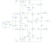
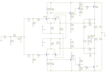
Add 2 diodes as below, and bias it in a such way that V(R13) is about 0.5v (>half of pn vdrop).
The idea is to clamp down the voltage drop across the sensing resistors before driven into class b, so that the opposite side never runs out of current.

Add 2 diodes as below, and bias it in a such way that V(R13) is about 0.5v (>half of pn vdrop).
The idea is to clamp down the voltage drop across the sensing resistors before driven into class b, so that the opposite side never runs out of current.
Last edited:

Yes, you know it ... "warm, süß und ölig" - we know it.The sound is overly warm, sweet and oily.
I had more than one A1 and I know what I´m talking about.
Rload please > 6 Ohm ever.
I'll just go on, now with the correct quiescent current for 20Wrms (which is set via the offset, i.e. the unbalance, but also via each individual resistor in the “LevelShifter” ...)
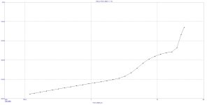
We know that frequency response compensation is hardly feasible - but let's play a little.


THD_1k:
5W = 0,001%
10W = 0,005%
15W = 0,03%
That doesn't look too bad, does it?
We know that frequency response compensation is hardly feasible - but let's play a little.
THD_1k:
5W = 0,001%
10W = 0,005%
15W = 0,03%
That doesn't look too bad, does it?
If you opt-in miller compensation, it will be much easier to compensate.We know that frequency response compensation is hardly feasible - but let's play a little.
Something can be done:
1. Add two miller caps.
2. Degenerate the input stage, so that you know how much the gm is, for compensation purpose.
3. Add current mirror to the input stage. As the bias current of the output stage has been taken care by the nfb, there is no fear of that the bias current would run away. You want the rest of amp to have as much gain as possible.
Last edited:
When you plot the THD it should be done with enough cycles otherwise the numbers will be truncated even if the simI'll just go on, now with the correct quiescent current for 20Wrms (which is set via the offset, i.e. the unbalance, but also via each individual resistor in the “LevelShifter” ...)
We know that frequency response compensation is hardly feasible - but let's play a little.
View attachment 1377800
View attachment 1377801
View attachment 1377802
THD_1k:
5W = 0,001%
10W = 0,005%
15W = 0,03%
That doesn't look too bad, does it?
time step is short enough.
Other than this compensation cant help improving the perfs, what you did here is to increase the IPS current and hence gain
but i dont think that it can yield 0.005%/10W, there s roughly one order of magnitude error here.
When you plot the THD it should be done with enough cycles otherwise the numbers will be truncated even if the sim
time step is short enough.
I'm relying entirely on @Bernhard here, he's “the MC-12 expert” of the two of us.
Other than this compensation cant help improving the perfs, what you did here is to increase the IPS current and hence gain
Doubled, that's right - and at the same time IC_Q10 and IC_Q8 set approximately equal, about 500µAdc. With the input offset current, this automatically leads to the correct quiescent current through Q7 ...
That may well be the case, but as you know, I don't believe in values that are much better than 0.03% in reality, i.e. that are verified by measurement.but i dont think that it can yield 0.005%/10W, there s roughly one order of magnitude error here.
#
However, the beautiful A1 has a weak point, especially if it is very strongly feed-back coupled, i.e. it also requires an input voltage of 4.5Vpp for the specified full modulation. Under no circumstances should this limit be exceeded!
How can we give the A1 the necessary operational reliability?
Attachments
Supplement
I don't want to encourage anyone to take their fully functional, original MF-A1 apart and tinker with it.
An original is and remains the original - but we can develop and build our own homage to “Tim & Antony”.
Musical Fidelity
HBt.audio
I don't want to encourage anyone to take their fully functional, original MF-A1 apart and tinker with it.
An original is and remains the original - but we can develop and build our own homage to “Tim & Antony”.
Musical Fidelity
HBt.audio
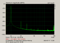
Simulation of the original A1
idle current 660 mA
THD
1W -67 dB
3W -62 dB transition from classA to classB
10W -44 dB
17W -41 dB clipping point
It can be said that distortion is quite high, resulting in the known sound coloration.
The dominant K2 and K3 give the sweet taste, which to some ears is still better than a bit harsh sounding amp, and may explain the success of the A1.
Also the simulation tightly matches the measurement of the amp.
Next post...
Attachments
Meine aktuellen ErgebnisseAlso the simulation tightly matches the measurement of the amp.
Next post...
not nearly as bad as the one you simulated - and by the way, it should be noted that the quiescent current is always around 800mA and not 600mA.
Dear Bernhard,I had more than one A1 and I know what I´m talking about.
would you do us Forians a big favor and make one of your many MF-A1s available for measuring purposes, or carry them out yourself?
I am interested in your measurement reports - and the question of whether you still like your n amount of MF-A1s? Or do you not have a single A1 in your garage at the moment?
#
If we now want to rely solely on simulation results, then it would be nice if you could work on a possible improvement of the A1 core.
After the common NFB (from the real output node), the only thing missing now is actually the attempt to successfully accommodate a current mirror, or to clarify whether a significant improvement can be achieved. "Zen Mod" has successfully considered the use of a HEX-Fet, as well as more negative feedback, a higher quiescent current (in line with the propagated 20W) and "better" output transistors -> virtually an IGBT replacement ..!
I take a slightly different approach.
Please work on this path successfully - and feed MC12. That would make me happy and maybe @m0rten will later work on a PCB for the forum.
greetings to munich,
HBt.

A1 demonstrates that how you could control the bias current through the NFB with the 2 complimentary LTP input stages. I would say this is brilliant.
My instinct tells me it would only work well with class A. Once one side of the output transistors runs out of current, the performance would suffer.
To come up a new design based on that, I would just use original output stage as VAS that only works in Class-A. Add a traditional output stage, such as EF2, after that.
The A1 bias scheme is perfect to create an alternative "VBE Multiplier" on the VAS. You get the idea.
Last edited:
brainstorming (without deeper thoughts) - could this quick and easy modification work "at all" ?

A1 demonstrates that how you could control the bias current through the NFB with the 2 complimentary LTP input stages. I would say this is brilliant.
My instinct tells me it would only work well with class A. Once one side of the output transistors runs out of current, the performance would suffer.
That's right 👍
Perhaps more classic after all?
If the simple current mirror brings salvation, the question now arises as to the optimum choice of transistor. The skeleton is in place, the choice of resistor values gives us some freedom, but which BJTs should we use to squeeze out the optimum?
For a "reboot" we should perhaps put all our eggs in one basket and go all out!
Any objections or cooperation?

not nearly as bad as the one you simulated - and by the way, it should be noted that the quiescent current is always around 800mA and not 600mA.
Zen Mod talks about 700mA in the other thread.
Maybe with other models it gives higher idle but that would not turn things around.
Dear Bernhard,
would you do us Forians a big favor and make one of your many MF-A1s available for measuring purposes, or carry them out yourself?
I had... long time ago.
Maybe the new A1 is a bit different and little better than the original.
My simulation @ 660 mA / 4V 0p in 8 ohms - Zen Mod measurement @ 700 mA - my schematic
K2 sim -68 dB, Zen Mod -70dB
K3 sim -77 dB, Zen Mod -80dB
K4 sim -96 dB, Zen Mod -100dB
K5 sim -101 dB, Zen Mod -105dB
MJ2955 changed to 2N2955:
-71 dB
-78 dB
-98 dB
-102 dB
Very close match
K2 sim -68 dB, Zen Mod -70dB
K3 sim -77 dB, Zen Mod -80dB
K4 sim -96 dB, Zen Mod -100dB
K5 sim -101 dB, Zen Mod -105dB
MJ2955 changed to 2N2955:
-71 dB
-78 dB
-98 dB
-102 dB
Very close match
Attachments
Last edited:
- Home
- Amplifiers
- Solid State
- An A1 descendant - a relentless analysis