MBK said:Or as seen from the Voltage gain, any distortion that is not part of the gain function A:
Vout=A*Vin+Dl1*Vin+Dl2*Vin+.... + Dn1 + Dn2...
=Vin(A+Dl1+Dl2+...) +Dn1+Dn2...
A=gain
Dl: linear distortion functions
Dn:nonlinear distortion functions
So for the linear part:
Vout1+Vout2=Vin1(A+Dl1+Dl2+...) + Vin2(A+Dl1+Dl2+...)
= (Vin1+Vin2)*(A+Dl1+Dl2+...)
For the nonlinear part:
Vout1+Vout2=Dn1+Dn2+.... <> (Vin1+Vin2)*(Dn1+Dn2+.... )
Example:
Harmonic distortion: linear (is a linear function of input)
Johnson noise, energy storage: non-linear, is independent of input.
Ahem. For lack of an "official" definition I inferred this myself from common usage of the terms...
For me, harmonic distortion is NON-linear distortion because it is caused by the NON-linear transfer function of the amplifying element. You put in sin(wt), and you get sin(2wt) out. Or sin(3wt), or...ad infinitum.
Jan Didden
As far as I remember, a system is by definition linear if it complies with the following requirement (superposition):
If an input signal x produces an output signal X and an input signal y produces an output signal Y, then an input signal ax+by should produce an output signal aX+bY, where a and b are constants, while x, y, X and Y can be (vector) functions of time.
I may have left out something about a zero element, but this is basically it. This means that most IC's in the so-called "linear" databooks are not even approximately linear. For example, the output voltage of a voltage regulator is only proportional to the input voltage if it is broken down. Offset, noise and harmonic distortion are all non-linear, frequency response errors are not.
Anyway, the misunderstanding about linear distortion is simply due to two different definitions of "distortion" being used. If you use a definition saying that distortion is by definition non-linear, linear distortion becomes a contradiction in terms.
Yes me too, when I'm saying distortion I mean normally non-linear distortion but this implies that any distortion is non-linear. So it's easier to say transfer curve or characteristic and distortion.
fdegrove said:
The explanation in this link is wholly misleading...distortion arising from 'uncorrelated' sources or otherwise, is simply distortion, and it is misleading to define such as 'linear distortion' and conversely.
Re: Amplifier topology objective effects
Andy or someone else, how do I get distortion values out of SwitcherCAD?andy_c said:The data for the single-ended amp was as follows:
Single-ended
-----------------
2nd harmonic: 61.3 dBc
3rd harmonic: 70.3 dBc
4th harmonic: 80.2 dBc
5th harmonic: 92.9 dBc
Complementary:
---------------------
2nd harmoinc: 69.6 dBc
3rd harmonic: 61.8 dBc
4th harmonic: 96.9 dBc
5th harmonic: 83.4 dBc
Total distortion is similar, but the assertions regarding improved 3rd harmonic distortion performance of the single-ended design seem to be correct.
The complementary design is shown below. I can provide the LTSpice projects if anybody is interested.
Hi P-A,
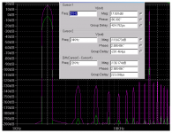
Set your source up for "sine" in the source properties dialog. I usually choose 12 cycles. You'll need to do an FFT, but on the last cycles of the waveform, since the first ones contain a transient that will make the results inaccurate. I usually choose the last 5 cycles. In the "simulate, edit simulation cmd, transient" tab, choose the "maximum time step" to be the time duration of 5 cycles, divided by (16384-1) since the default FFT has 16384 points (so there will be 16383 steps). Next go into tools, control panel and disable all compression on the compression tab. Perform the transient analysis. Right-click on the graph and choose "FFT". In the resulting dialog, choose "specify a time range". For example, with the last 5 cycles of a 12 cycle total simulation at 20 kHz, pick 350 uS and 600 uS for the start and stop times. If you were to choose "use extent of simulation data" here, the FFT would include the initial transient, increasing the measured distortion. Click Ok and you'll have your plots. They come out in dBV, (20 * log(VRMS/1VRMS)) so you may want to scale the data so its scaled peak value is sqrt(2) Volts, giving 0 dB for the fundamental.
Set your source up for "sine" in the source properties dialog. I usually choose 12 cycles. You'll need to do an FFT, but on the last cycles of the waveform, since the first ones contain a transient that will make the results inaccurate. I usually choose the last 5 cycles. In the "simulate, edit simulation cmd, transient" tab, choose the "maximum time step" to be the time duration of 5 cycles, divided by (16384-1) since the default FFT has 16384 points (so there will be 16383 steps). Next go into tools, control panel and disable all compression on the compression tab. Perform the transient analysis. Right-click on the graph and choose "FFT". In the resulting dialog, choose "specify a time range". For example, with the last 5 cycles of a 12 cycle total simulation at 20 kHz, pick 350 uS and 600 uS for the start and stop times. If you were to choose "use extent of simulation data" here, the FFT would include the initial transient, increasing the measured distortion. Click Ok and you'll have your plots. They come out in dBV, (20 * log(VRMS/1VRMS)) so you may want to scale the data so its scaled peak value is sqrt(2) Volts, giving 0 dB for the fundamental.
Thanks, many buttons and tabs..
Now I have exercized (spelling?) but I get too fantistic dist values of the basic CFB amp, -115 dB!
Now I have exercized (spelling?) but I get too fantistic dist values of the basic CFB amp, -115 dB!
Another way to get to FFT, from the toolbar select View>FFT when you are in the plot window (don’t you hate it when the tool bar menus are context sensitive? You can’t even see what’s available if you don’t start in the right place)
The FFT dialog box has many options:
Time - I used 6mS START to 10mS END in the plot below
Data Sample points = 65534
Smoothing Filter Points = 1
Window = none
While it seems more data points in the simulation file (controlled by maxstep .TRAN option) would be better, the FFT plot does seems to mess up with more data points in the time interval than FFT data points, the Binomial Smoothing Filter seems to help this (just increase filter length until you get reasonable resolution in FFT, remembering that you are FILTERING the data) and I haven’t found Andy’s exact calculation of time step setting in .Tran necessary
When you get the plot looking like what you want [PLOT SETTINGS] , saving the plot settings in a file lets you repeat the plot for multiple circuits with the same signals and scales to more easily compare
(the plot below is for the modified “Lin” style amp I show in post 149,150 page 10 of this thread with d1 bypassed with 1 mF, posts 169, 183 give a little more info on circuit&SwCad FFT plot – as you can see I’m still learning the SwCad tools too)
(rt clik on signal in FFT plot to get dialog box to enable both cursors, cursor 1 turns on when you left clik signal, cursors drag, last cursor moved will be moved by right,left arrow key to FFT data point, dragging leaves you at fractional locations)
Low distortion # aren’t really a challenge with high loop gain and I show simple modifications that give ridiculously high gain with a simple topology, Baxendall’s Super Pair is as great a bargain as Cherry’s moving the compensation C to the output
Attachments
jcx said:........Baxendall’s Super Pair is as great a bargain as Cherry’s moving the compensation C to the output
Hi jcx....
(1) Can yu show your schematic of amp. using Baxandal's super pair?
(2) have you actually built and used an amp. with the output stage inclosed within the miller minor feedback loop...a la Cherry?
...if so, was it stable?
I think the Super pair should rank up there with cascode (to which it is closely related) and the CFP/Sziklai compound transistors, with Baxendall, Hawksford and Carr vouching for its utility it is hard to understand its obscurity
Ref in http://www.diyaudio.com/forums/showthread.php?postid=159617#post159617
Jcarr’s reply a little further down: http://www.diyaudio.com/forums/showthread.php?postid=159709#post159709
Circuit examples in:
http://www.diyaudio.com/forums/showthread.php?postid=204778#post204778
Q6,8 and Q7,5 R3 is a simple shared “current source”
http://www.diyaudio.com/forums/showthread.php?postid=209401#post209401
Q11,3 again R15 is a cheap current source bias
Re Compensation;
Designing precision instrumentation electronics I haven’t tried compensating power output stages in a long while, I have used small signal/medium power transistors in op amp feedback loops as followers and gain stages so I feel pretty confident that the simulations represent workable circuits – the LT1028 is compensated this way, and Cherry would claim the many CE output stage devices (AD823 and 8027 are two I’ve looked at recently) count as equivalents from a stability standpoint: “Output Resistance and Intermodulation Distortion of Feedback Amplifiers” JAES, V30#4 April ’82 p178-190
Cherry has pretty baldly challenged anyone to bring counterexamples or analysis of his compensation recommendation to his attention, and repeated this for over a decade without any published refutation that I’ve seen, do you have any such reference or evidence? “IRONING OUT DISTORTION” in Electronics World + Wireless World (1/95, and 7/97 issues)
I must admit I am amazed that class B power stages can be compensated by any means given the wide swing in operating point and small signal bandwidth during crossover – the class A, deep class AB circuits with fast small signal/medium power transistors I’ve simulated are a best case
jcx said:Baxendall’s Super Pair is as great a bargain as Cherry’s moving the compensation C to the output
After seeing your earlier post referring to the Baxandall super pair and the Hawksford cascode, I ordered the Hawksford AES article (as well as Cherry's distortion analysis article). I did a simulation of the Baxandall super pair in a complementary power amp with +/- 90 Volt supplies, at 20 kHz with a voltage swing corresponding to 300 W into 8 Ohms if a speaker were connected. The output stage was just an ideal VCVS with unity gain just to see the input stage and VAS distortion contribution. First stage transistors of the super pair were 2N5401 and 2N5551, and second stage were MJE340 and MJE350. All were running at a DC current of about 5 mA. Global feedback factor was a low 17 dB. I got results with the super pair that were no better than a conventional cascode with fixed DC voltage at the base of the common base amp. However, when I tried the Hawksford cascode, I got a 20 dB improvement over the conventional cascode, in line with what Hawksford saw in his measurements. So I was quite happy with the Hawksford cascode, and rather puzzled with the performance of the super pair. Compensation was a simple Miller capacitor that did not enclose the output stage. Then I tried an emitter follower inside the Miller integrator loop with the Hawksford cascode and got an additional 10 dB reduction. Previously, the EF had negligible effect, as the distortion must have been dominated by the slope distortion from the conventional cascode. Needless to say I'm quite pleased with these improvements and glad I took jcx's suggestions about the Hawksford article.
andy_c said:
Then I tried an emitter follower inside the Miller integrator loop with the Hawksford cascode and got an additional 10 dB reduction.
...such an arrangement may be prone to intractable local instability in practice...ie..emitter follower driving cascode, all inclosed in miller minor loop...
mikek said:...such an arrangement may be prone to intractable local instability in practice...ie..emitter follower driving cascode, all inclosed in miller minor loop...
Yes, I remember your earlier post on this in the Slone amp thread. The article I got from you (thanks BTW) didn't seem to have info on this though. It was the survey of amplifier architectures article. One author was Witulski, I think, I don't have it handy. So I think the analysis of this must be in some different article? Anyway, I'm going to look into this using the Middlebrook technique for computing loop gain and phase, using just the local Miller integrator loop for signal injection. When I finally get around to finishing the design and get boards made, it should be simple to jumper around the EF if problems arise in practice.
As an aside to the other discussion concerning putting the output stage inside the Miller loop, it looks like the LM3875 ("gainclone") does this. I wouldn't do this myself though, as I'm trying to get the best possible stability into capacitive loads without an output inductor.
The Super pair wins big as a VAS stage because it nearly equals the cascode on the output while increasing the input impedance, boosting the gain when driven with a current mirror. If you drive it from a collector resistor, I’m not surprised you didn’t see a big difference.
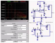
Simplest comparison I could come up with shows > 100x distortion improvement as a VAS over a single Q:
Simplest comparison I could come up with shows > 100x distortion improvement as a VAS over a single Q:
Attachments
mikek said:
Hi jcx....
(1) Can yu show your schematic of amp. using Baxandal's super pair?
(2) have you actually built and used an amp. with the output stage inclosed within the miller minor feedback loop...a la Cherry?
...if so, was it stable?
Hi mike
I tried that whit my self blameless... it was fairly stable...
It didn’t gave any improvement in the null test and for me it wasn’t worth the risk...
And one more thing, the miller cap creates a direct path at high frequencies, so all the HF garbage pick up by your loudspeaker cables will be directly injected on the VAS and it will most probably overload...
So for me it isn’t worth the risk
Regards
I will try that one again on my NE5534 clone amp and i will report back...
jcx said:The Super pair wins big as a VAS stage because it nearly equals the cascode on the output while increasing the input impedance, boosting the gain when driven with a current mirror. If you drive it from a collector resistor, I’m not surprised you didn’t see a big difference.
Simplest comparison I could come up with shows > 100x distortion improvement as a VAS over a single Q:
Okay, I also have a sim set up at home of a Lin topology with the same transistors, power supply voltages etc. as I described for the complementary amp (including unity gain VCVS instead of output stage). It has the Hawksford cascode, and a current mirror output for the diff pair. Should be a simple matter to compare the super pair with the Hawksford cascode when I get home this evening. I seem to remember doing this already, with similar results to the complementary amp, but I'll double-check to be sure. If you're interested, I can post the LTSpice files so you can verify the results for yourself.
Please, do so. I have fooled around more with LTSpice and it takes some time to get used to it. The user interface isn't winning any rewardsandy_c said:I can post the LTSpice files so you can verify the results for yourself.

rickpt said:
I will try that one again on my NE5534 clone amp and i will report back...
Hi Rickpt,
NE5534 is a good op amp....uses Johan Huising's nested miller compensation, together with a feedfoward path around the second stage...
...problem with the later, is that it generates a pole-zero doublets before unity-gain cross-over, which increases settling time.....
...this however, is unlikely to be of great significance in an audio power amp. with an output inductor fitted, as delayed settling resulting from normal ringing with said inductor is likely to swamp the effect of the doublet...
- Status
- Not open for further replies.
- Home
- Amplifiers
- Solid State
- Amplifier topology subjective effects