You are forgetting that not all of the 100 ohm will be in use. It is an adjustable resistance after all. My simulation suggest
That's what I don't get. I was starting from the fact that we have 4 junctions, 2 on each side, being fixed mostly by the diodes, plus the 0.22 resistors. Starting from that, and using 0.7V as typical drop, I get 2.8V and maybe a tiny bit more. If we use 0.6V per junction, we're at 2.4V. Anyway, the way I figured, if we have those 2 BCs causing 2 junctions of drop, then there would be about 2 junctions worth left on that spreader pot.
about 20% of that 100 ohm, i.e. 20 ohm * 8 mA = 160mV of voltage drop across the pot. Add it to the ~650mV across each diode-connected transistor and you are in the ballpark of 1.5V.
That's what I don't get. The 2 BCs causing 2 junctions drop, plus a bit more from 20% of full value on that pot, and we're not even close to the 4 junctions we need to spread.
So I'm still missing something...
The bias network is OK, but a Vbe multiplier would work better.
I agree, and that would be more reliable, because we can make sure the pot's wiper, if it doesn't connect, would cause the bias to drop instead of going higher.
Plus a TO126 can be fitted on the heatsink for better tracking, probably better than those TO92s thermally coupled and not on the heatsink.
That heatsink, with its 200mm length, is very crowded already with the 6 TO3s plus the 2 TO220s, so it would be quite a feat to jam one more TO126 in there...
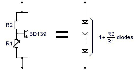
The current through the BC639 and 640 is in the order of 1 mA. They have 100
R resistors connected which make for 600 + 100 + 100 + 600 mV = 1.4 V
total bias voltage + whatever you get from the emitter R's of the outputs.
I thought we had 4 junctions of spread there and that the 4 diodes would keep that there, but I just realized they're in reverse, so I was wrong about that.
But that "super" darlington we have with the 3 transistors forming one (sort of), doesn't that cause at least 2 junctions to be seen from the base?
I would like this better than those 2 BCs actually. Even if it causes a little issue fitting that extra TO126 on the heatsink. It seems like a more practical solution.
What would work best?
I was searching for non polarized caps for the 10u on the feedback and there aren't that many choices in this type of value.
Most are quite expensive and they're polarized anyway. The tantalum would be nice if non polarized.
I found a ceramic type, multi-layered:
http://www.mouser.com/ds/2/400/leadmlcc_commercial_midvoltage_en-253021.pdf
There is a 10u in 100V radial with 5mm lead spacing. This seems like a good choice, and it's among the cheapest in that capacity and non polarized.
Two 4.7uF wima mks2 in parallel could be a possibility. Not that expensive at Reichelt.
What suppliers are you considering ?
What suppliers are you considering ?
Two 4.7uF wima mks2 in parallel could be a possibility. Not that expensive at Reichelt.
That one is at less than 1euro a piece if buying at least 10 units at mouser.
We're now tight for space on that pcb, so using radial parts and only one piece is a must to save on space.
What suppliers are you considering ?
Looking at many: mouser, digikey, futureelectronics, buerklin, etc...
Here are the latest sch.
I'm pondering changing the C1 input cap for something bigger, like 2.2u or 4.7u, maybe even the same 10u as the bipolar in the feedback.
This would lower the cut off of the input high pass, would still block any DC. But does this require altering the values on the resistors R2, and maybe R3?
R1 needs to stay at 100k to match R5 on the main feedback and doesn't fix the input impedance as well?
I ended up removing those additional decoupling caps from the output's power pins, I think I was just wasting them there.
Attachments

Looking at my junk in stock, I don't have any BC546/556 types, only a few 557 and tons of the 547. I'm thinking about using mpsa42/92 instead.
I was comparing the mpsa42/92 with the bc639/640 and they're very similar except for the high voltages on the mpsa. However the 639/640 can handle more current and that was why it was chosen in the first place as a predriver, so I won't use the mpsa in those positions.
I'll have to locate a few parts, but most of it I do have.
There are also the big filter caps. I used 10mF in the sch, the 80V should do, and I provided for 40mm diameter on the pcb, so there are choices. Is there a good source for those? (cheap, but good that is)
Look at this article by Rod Elliott for a very good bridging arrangement.
Simplest Ever Bridging Adapter for Amplifiers
Simplest Ever Bridging Adapter for Amplifiers
Look at this article by Rod Elliott for a very good bridging arrangement.
Simplest Ever Bridging Adapter for Amplifiers
Yes, using the feedback from one to drive the opposite one, it's roughly how power does this in their amps, such as the apk4500 for example (I have one of those).
What we're aiming for is more complex for sure, and it's based on the crown/amcron design.
I thought we had 4 junctions of spread there and that the 4 diodes would keep that there, but I just realized they're in reverse, so I was wrong about that.
But that "super" darlington we have with the 3 transistors forming one (sort of), doesn't that cause at least 2 junctions to be seen from the base?
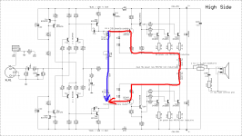
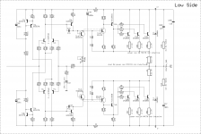
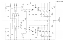
As far as bias voltages and currents go, you only need to look at the ones indicated by the arrows in my picture. The voltages along the blue line adds up to the same value as that along the red line. Each has two Vbe drops. The pot is adjusted to have the same voltage across it as the sum of those across R26, R27, REHA and REHB.
The transistors T15 to T22 are not thermally tracked by the bias network. It is a feature of the design that you have chosen. This can be a good thing or a bad thing, depending on who you ask.
Attachments
Last edited:
Looking at my junk in stock, I don't have any BC546/556 types, only a few 557 and tons of the 547. I'm thinking about using mpsa42/92 instead.
I was comparing the mpsa42/92 with the bc639/640 and they're very similar except for the high voltages on the mpsa. However the 639/640 can handle more current and that was why it was chosen in the first place as a predriver, so I won't use the mpsa in those positions.
When trying to select a small-signal transistor to use, you could look at the graphs of DC current gain against collector current in the data sheets. The flatter the curve, the less distortion there will be.
As far as bias voltages and currents go, you only need to look at the ones indicated by the arrows in my picture. The voltages along the blue line adds up to the same value as that along the red line. Each has two Vbe drops. The pot is adjusted to have the same voltage across it as the sum of those across R26, R27, REHA and REHB.
The transistors T15 to T22 are not thermally tracked by the bias network. It is a feature of the design that you have chosen. This can be a good thing or a bad thing, depending on who you ask.
Ok, now I get it. But I'm still thinking it wouldn't be a luxury to tweak this for a more reliable setup in case the wiper loses contact. I'm not hot on using fixed resistors and solder them on the board to tweak the bias.
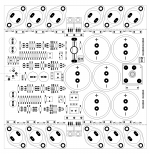
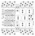
Here are the latest sch and I attempted a parts layout as well.
One thing would be interesting to find out, by simulations, is if we took the feedback from the other side of the output L//R instead, would that change anything about the distortion? Would it affect anything else? output impedance? damping factor???
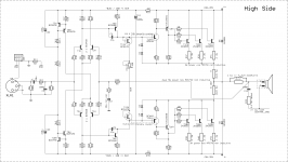
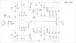
See what I mean on the latest high side sch. I will put it back to normal after that if there is no improvement from moving the feedback that way. But it seems logical that including the output coil inside the feedback loop would improve distortion. This doesn't apply to the low side of course.
One thing would be interesting to find out, by simulations, is if we took the feedback from the other side of the output L//R instead, would that change anything about the distortion? Would it affect anything else? output impedance? damping factor???
See what I mean on the latest high side sch. I will put it back to normal after that if there is no improvement from moving the feedback that way. But it seems logical that including the output coil inside the feedback loop would improve distortion. This doesn't apply to the low side of course.
Attachments

I would not place the R||L on the amplifier PCB.
It should go into the cable route to the output socket/terminals.
When located there, it becomes obvious that the NFB tapping should remain on the PCB before the R||L.
It should go into the cable route to the output socket/terminals.
When located there, it becomes obvious that the NFB tapping should remain on the PCB before the R||L.
I would not place the R||L on the amplifier PCB.
It should go into the cable route to the output socket/terminals.
Ok, so then the zobel also goes off board.
When located there, it becomes obvious that the NFB tapping should remain on the PCB before the R||L.[/QUOTE]
Make sense. I wonder how this affects performance though.
The schematic will no longer show the high side zobel and R//L. I'll have to use some other type of connector for the output, as the taps are on opposite side of the board and we don't want to have those tracks travel across the board too much. The wires will of course have to travel separately for a while, but in the air, and then they can be twisted before going to the real output plug and have the R//L and zobel soldered there.
Thanks for your input.
Spookydd,
Congratulations. Perfect PCB layout. One minor point though. I understand
that you are planning to drive this amp hard. In that case, maybe the bridge
rectifier is better placed off-board on the chassis for cooling purposes. This
way, you will get a little bit more space on the most expensive real estate
in the world.
Could I have your postal address please ? Tomorrow (Monday) I am planning
to visit the post office for everybody else interested in the PCB.
Cheers
Selim
One minor point though. I understand
that you are planning to drive this amp hard. In that case, maybe the bridge
rectifier is better placed off-board on the chassis for cooling purposes. This
way, you will get a little bit more space on the most expensive real estate
in the world.
I chose a 35A GBPC-W, for the wires so it can be easily soldered on the board and 35A should be able to handle everything we can throw at it, and probably without breaking too much of a sweat. However I did think about some cooling and I was thinking a small heatsink can be slapped on top of it. But there again, we need to calculate how much heat that thing will generate and you may be right that it may need a bigger heatsink than I thought and moving it off board could help that.
The main reason I wanted it on the board was to reduce wiring as much as possible.
How much heat can we expect from it? I haven't calculated this type of device's dissipation before, that would be a good start. What do I start from? The drop on the diodes?
Could I have your postal address please ? Tomorrow (Monday) I am planning
to visit the post office for everybody else interested in the PCB.
Ah! That means you didn't receive my email. I may have done a typo, but it didn't come back yet.
I'll try using the forum's private messaging system then.
Here are updated sch and layout.
The removal of the R//L and zobel provided some breathing room so I could spread parts some more and I am aiming at a clearance of 20mils in the design rules. Having also previously removed many extra decoupling caps, I now have enough room. Some room will be needed to add the circuitry still missing to bridge this properly.
I'm still moving and swapping parts on the layout a bit, to make it more routable, and I've been doing quite a bit of routing already, although it's quite far from finished.
There is more work on the sch to make it a grounded bridge. What's next?
Attachments
Here is one idea to keep the bridge on the pcb and allow a big enough heatsink to be put on it: How about putting it on the solder side of the board? That way it can easily be fitted with whatever heatsink we can come up with.
The board would not be close to a case below on its solder side, since the heatsinks raise the board well above that level because of their flanges half way up.
I was giving some thoughts to the bridge's dissipation. Tell me if my reasoning is wrong, but first we don't need to add the dissipation of all 4 diodes. I think we just need to look at rms dissipation on half of the bridge only. Am I wrong on this?
Then the datasheet is a bit ambiguous to me, providing a thermal resistance as "junction to lead" and not "junction to case". It calls for a 1.5K/W and total dissipation of 83.3W. The forward current derating curve shows the GBPC35 good for 35A for ambient temperature over 50C. I understand this as without a heatsink (Am I wrong here?).
The forward drop is also not very clear to me, as they state 1.1V "per bridge" and not "per diode". I doubt the forward drop of one diode would only be 0.55V, so I guess we have to interpret this as per diode.
I this case, taking the worst case of one amp seeing a 2ohms load (from a 4ohms bridged load), at full power, with an output voltage (on the load) probably not more than 20Vrms, assuming the losses aren't too steep. Then we're at somewhere around 10A of rms current. In one diode, we would have a little over 10 watts of heat to dissipate, times 2 for the bridge. Correct?
- Home
- Amplifiers
- Solid State
- Amplifier based on 2N3055