You do like circuits with multi-way feedback connections (to the VAS, to the Input and to the OPS) that really make me think😉
But am relaxed about this one because the response in this loop is "textbook".
In particular, the phase looks pleasantly understandable, just simple minimum phase.
Yes, I do. I like to try and do things differently. Keeps me (us) interested. 😉
Thought the phase response resembled the one we saw in my other amplifier with HEC. So I thought it looked ok. The compensation has not really been tuned but was just thrown out there as a concept.
We know that feed-forward can potentially produce RHP zeroes, in other words "excess phase", in the strict use of the term.
So if there is no evidence of excess phase then I assume the feed-forward is so small that a simple analysis is fine and the complication of a Middlebrook GFT analysis is not needed.
On your post #48 you showed the shunt VAS loop to look for feed-forward there.
I think there is just a trace of non-minimum phase there, based only on visual estimate.
A second "To Do" is to work out how to plot excess phase in LTSpice.
In this case not critical because the loop gain is always small.
So using slightly dodgy logic. There may be a trace of feed-forward in the shunt too. Looking at the circuit, I wouldn't be too surprised. 😉
We learn about some loop no matter where you put it.😉
True. Hopefully this one showed the feed-forward.
Yeah! My own development example has MIC and no front-end shunt.
So my recommendations naturally tend to lead in that direction.
But I hope you will find that it does perform better on objective metrics.
That would confirm that it's simply a better idea and not just my prejudices that have mislead you.
Best wishes
David
My decision to use MIC was only slightly biased by your recommendation. Using a zero in the feedback network (cap across feedback resistor) seemed sub optimal and a form of MIC looked like an obvious solution. At high frequencies hopefully it provides a short cut back to the front end summing node.
Yes, in this instance MIC has improved virtually every spec of this amplifier especially slew rate and stability. THD stayed about the same.
One downside to this amplifier's compensation is that it is difficult to make it symmetrical. Especially the shunts.
Paul
...Hopefully this one showed the feed-forward.
Yes, I think so.
Just to confirm, when I said the response was "textbook" I meant this loop.
So if it has a textbook minimum phase response then feed-forward is not an issue.
Actually the other loop is pretty textbook too.
And you can easily put back the front-end capacitors to add a little PM if you need it.
When I did simulations on my (similar-ish) amp I was surprised to see how much of the PM was eaten away once I started to put capacitive loads and pushed the OPS transistors up near the rails to test under low Vce.
So the PM that I expected to be conservative turned out to be adequate but not by too much.
My decision to use MIC was only slightly biased by your recommendation. Using a zero in the feedback network (cap across feedback resistor) seemed sub optimal and a form of MIC looked like an obvious solution.
They are not mutually exclusive.
I like to use MIC and also the zero in the feedback loop too.
Yes, in this instance MIC has improved virtually every spec of this amplifier especially slew rate and stability. THD stayed about the same.
Nice both to have my own experiences confirmed, and to have been able to contribute.
MIC certainly can improve slew rate.
The stability/THD is usually a trade off, one can improve one or the other, or both a little bit.
I suspect that in your case there is not so much "spare" gain so it's stability that improves mainly.
One downside to this amplifier's compensation is that it is difficult to make it symmetrical. Especially the shunts.
Yes, this sort of duplication bothers me a little, on principle even when I can't see a specific problem.
I have no shunts and I use two Pole MIC from the centre point of the bias spreader to eliminate even the possibility.
You could probably use similar ideas, in my case it complicated the bias spreader just a little.
Perhaps JCX and Scott Wurcer would consider this excessive attention to mere visual symmetry.
My response is that it helps me be sure that stray inductance and capacitance can be balanced or cancelled in the PCB layout.
Similar issue in some of the CFB circuits and a few variations of capacitor placement have been shown, one by Damir.
Best wishes
David
Last edited:
Yes, I think so.
Just to confirm, when I said the response was "textbook" I meant this loop.
So if it has a textbook minimum phase response then feed-forward is not an issue.
Actually the other loop is pretty textbook too.
And you can easily put back the front-end capacitors to add a little PM if you need it.
Good, good, that 3 hours spent trying to understand probe placement was a good investment. 😉
It resembled the HEC amplifier in phase response which was seen to be ok. So in my limited knowledge thought it looked ok.
Probably leave the front end caps out as less components means an easier PCB layout.
When I did simulations on my (similar-ish) amp I was surprised to see how much of the PM was eaten away once I started to put capacitive loads and pushed the OPS transistors up near the rails to test under low Vce.
So the PM that I expected to be conservative turned out to be adequate but not by too much.
Tried torture testing this amp in sims with pure capacitive load with a small square wave super imposed on a 1K sine wave into clipping. It rang but didn't break away into uncontrolled oscillations.
How can you trick LTSpice into giving Loop Gain plots for when the output is close to the rails?
They are not mutually exclusive.
I like to use MIC and also the zero in the feedback loop too.
Had thought about this but managed to control myself. 😉 And now you say you use this method....
Yes, this sort of duplication bothers me a little, on principle even when I can't see a specific problem.
I use two Pole MIC from the centre point of the bias spreader to eliminate even the possibility.
Perhaps JCX and Scott Wurcer would consider this excessive attention to mere visual symmetry.
My response is that it helps me be sure that stray inductance and capacitance can be balanced or cancelled in the PCB layout.
Best wishes
David
It bothers me as well as... One problem I have with this amp is that the pre drivers are folded so there isn't a natural point to tap off centrally without duplication of compensation components.
Don't want to tap off the VAS for the MIC as I want to have the shunts as the main loading only. These shunts are complicated enough already.
Agree with the balancing of parasitics. No symmetrical amp is really symmetrical....
Another point to note, have noticed, in this amp the OPS zobel values are important and do make a difference to stability.
Paul
P.S. I do enjoy these discussions. Thank you. 🙂
Edit: Due to cross post. MIC brings gains without apparent drawbacks as long as you match the point where the shunt gives max attenuation to the point where the feed-forward path peaks in gain. Which seems sensible to me.
Last edited:
Probably leave the front end caps out as less components means an easier PCB layout.
Sure. I am a minimalist😉
But these ones have a pretty simple connection, maybe do the board so they can be done point to point if tests show a benefit in practice, the transistors should be only millimetres apart anyway.
How can you trick LTSpice into giving Loop Gain plots for when the output is close to the rails?
This is one of those tricks that is so simple that you'll say "d'oh!"
It's a DC coupled amp so just add a DC offset to the input of the LTP😉
Then you can check the stability quantitatively, even near clip.
Much better than eyeball "it doesn't oscillate too badly"
...And now you say you use this method...
I'm just a wannabe mathematician, don't trust me!
I do enjoy these discussions.
Me too, thanks, and it helps me to put my ideas into written form.
I hope to restructure some of this for Linear Audio.
Best wishes
David
Last edited:
Sure. I am a minimalist😉
But these ones have a pretty simple connection, maybe do the board so they can be done point to point if tests show a benefit in practice, the transistors should be only millimetres apart anyway.
Good point and the Supertis front also by its nature looks fairly straight forward to layout.
This is one of those tricks that is so simple that you'll say "d'oh!"
It's a DC coupled amp so just add a DC offset to the input of the LTP😉
Then you can check the stability quantitatively, even near clip.
Much better than eyeball "it doesn't oscillate too badly"
D'Oh. Have to try this later. Don't like not being able to analyse something properly. 🙂
I'm just a wannabe mathematician, don't trust me!
I'm just a wannabe amplifier designer 😉
In all seriousness, you have freely shared your knowledge to help me which is much appreciated.
Me too, thanks, and it helps me to put my ideas into written form.
I hope to restructure some of this for Linear Audio.
Best wishes
David
Mutual beneficial relationship. 🙂
It's good to try ideas and tie up concepts. And then to try prototypes...
Are we due for part 3 in the next edition?
Paul
Tried the LTSpice input offset trick...
It appears the current .asc setup (104 degrees PM and 27 dB GM) can just about tolerate a 0.2R + 100nF as a load (PM = 5 degrees, GM =0.3 dB),This is while being 2V off clipping.
Found another place to gain some PM bypassing the current source resistors. 😉
In this amp it is the input stage that clips first. Which is maybe why it clips so cleanly. It also means that the output transistor Vce never falls anywhere close to 0V so PM not compromised so much (if at all) by the voltage swing of the amp.
Tried the LTSpice input offset trick...
Nice that it seems to have been useful.
The square wave on a sine method (R.C.Bowes I think) is fine for tests of real hardware.
But then there seems to have been a sort of mental set and the same technique was transferred to LTSpice.
So when I came up with the bias method I went "D'oh" that it hadn't occurred to me immediately, when it was both simple and more informative.
The actual data made me a bit shocked to see how much the nominal stability PM was eaten up as the amplifier moved to the rails.
That's part of the reason I liked the front end zero capacitors, they provided some extra leeway.
But my development version has elevated front end rails so your results are not quite comparable.
I will have a think about current source bypass capacitors, maybe useful in my dev. version too.
Best wishes
David
Last edited:
Nice that it seems to have been useful.
The square wave on a sine method (R.C.Bowes I think) is fine for tests of real hardware.
But then there seems to have been a sort of mental set and the same technique was transferred to LTSpice.
So when I came up with the bias method I went "D'oh" that it hadn't occurred to me immediately, when it was both simple and more informative.
The actual data made me a bit shocked to see how much the nominal stability PM was eaten up as the amplifier moved to the rails.
That's part of the reason I liked the front end zero capacitors, they provided some extra leeway.
But my development version has elevated front end rails so your results are not quite comparable.
I will have a think about current source bypass capacitors, maybe useful in my dev. version too.
Best wishes
David
Hi David,
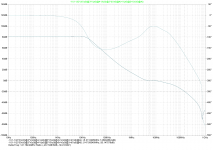
It is interesting to see how much PM you really need. Have been experimenting with TPMIC or at least my version... Again, THD showed almost no change but stability margins were very much improved. Something like PM = 116 degrees and GM = 26 dB @ULGF 7.5MHz.
Is 116 dgrees enough? Is 7.5Mhz ULGF asking for trouble?
PCB layout will be critical to this amp. It seems to always want to run fast in sims. Probably be the same in reality... On that note a plan a second prototype only this time actually paying attention to layout. 😉
And the current limiters will have to go. Lends itself to a solid state relay like Bonsai documents on his website. The current limyers cost PM. Not immediately obvious to me but when you consider that the diodes (D5, D6) are really 4pF capacitors. Another benefit of the solid state relay is that you could choose a MOSFET with Rds ON of at least 0.4R and do away with the output network? Trade one source of distortion for another. 😉
I like the square wave on sine method in LTSpice. Just with a little difference. At least with my HEC amp you could use the current in the gate resistor to see the first signs of instability long before you can see it on the output of the amp.
And you win on the input stage bypass caps by the way. 🙂
Paul
P.S. This amp has now surpasses my previous CFA attempt in every way. 🙂
Hi Guys
Just a Q about current sources used in CFAs:
The feedback type CS using a small BJT to monitor current via the Re of the pass device is generally faster and more linear than the "buffered references" used here and by others - I don't really think of them as proper current sources. Apart from simplicity of drawing, why does everyone use these simple CSs? I always use the two-BJT type when I need a CS.
In a CFA or diamond, it is the CS that turns on the next stage. To do it fast requires a fast CS. For this reason also, I disagree with the common notion that "current sources are not a part of the signal path". In a CFA where speed is desired, it would seem that a better CS would be "a good thing".
Even the two-BJT CS can be sped up if necessary.
Have fun
Hi Guys
Just a Q about current sources used in CFAs:
The feedback type CS using a small BJT to monitor current via the Re of the pass device is generally faster and more linear than the "buffered references" used here and by others - I don't really think of them as proper current sources. Apart from simplicity of drawing, why does everyone use these simple CSs? I always use the two-BJT type when I need a CS.
In a CFA or diamond, it is the CS that turns on the next stage. To do it fast requires a fast CS. For this reason also, I disagree with the common notion that "current sources are not a part of the signal path". In a CFA where speed is desired, it would seem that a better CS would be "a good thing".
Even the two-BJT CS can be sped up if necessary.
Have fun
Hi Struth,
From my perspective, it's not so easy. Depends on particular requirements. For example, in many cases, a two-BJT CS is less temperature-stable, than a simple one with LED as a reference. Also, speed very much depends on particular transistors used.
Cheers,
Valery
...how much PM you really need...116? Is 7.5Mhz ULGF...trouble?
This is the crux question, isn't it.
I have read comments that 7.5 MHz is well past a safe ULGF, no matter what the simulated PM.
But I don't believe it.
I suspect people had what they considered conservative stability and when the amp oscillated then they assumed there was some practical limit.
Instead the problem was simply that they had not simulated properly.
As I said, I was shocked to see how the PM disappeared as my amp neared the rails.
Unless I had done this then I would have been quite mistaken in a belief that the amp had plenty of PM.
The traditional 2 uF load test may also have mislead people
The worst case is usually quite different, your result of 100 nF is in line with Self comments (and Ric Lee's IIRC).
I don't have a particular number, because amps differ, for instance my amp's elevated front end supply can push the OPS close to the rails, your amp may have other critical areas.
PCB layout will be critical to this amp. It seems to always want to run fast in sims. Probably be the same in reality... On that note a plan a second prototype...
Theory implies that an increase in ULGF can improve stability, if properly done.
I think that's what you see when you say it wants to run fast, and I expect this is indeed the same in reality.
But layout will be important. Most DIY layouts are fairly sloppy and there is plenty of room for improvement.
I do have a layout that simulates at least 10x lower inductance.
If sloppy layout works OK at 2 MHz ULGF then a smart layout should be OK at 7.5 MHz.
PCs run at thousands of MHz with ordinary PCB materials and components, just attention to layout practice, so we are very, very far from limits.
Second prototype sounds a fine idea. You can see if my ideas on layout make sense.
Lends itself to a solid state relay like Bonsai documents on his website... Another benefit of the solid state relay is that you could choose a MOSFET with Rds ON of at least 0.4R and do away with the output network?
I like the idea of MOSFET protection and Andrew has done some nice work for this.
I did notice a failure mode if the output is shorted to earth and raised this with him.
He feels that this is not sufficiently likely to warrant a rework.
That is not unreasonable, but I plan to do it a little differently in my amp and switch the power amp main rails.
This not only protects the speaker but also can protect the OPS far better than fuses.
It has the feature that it completely removes the Mosfets from the audio path.
Not that I think this makes any audible difference, it just preempts even the most obsessive critics.
And you win on the input stage bypass caps by the way. 🙂
I don't win, hopefully your amp wins😉
Small bypass capacitors are so cheap and reliable, and they fit so simply and neatly into this layout that they seem a natural for a performance amp like yours.
But simpler amps are nice too.😉
Just need the compensation a little heavier.
Best wishes
David
...The feedback type CS ... faster and more linear than the "buffered references" used here and by others...
why does everyone use these simple CSs?
As my comment to Paul implied, I haven't yet considered current sources that much, so this interests me.
Why do you think the feedback source is "faster"?
I am a keen feedback fan but there are always issues of stability and frequency response peaks to consider.
I have looked at the somewhat equivalent case of Emitter Follower assisted Current Mirrors and they can definitely hit the stability of circuits that use them.
Bob Cordell has also commented on this as the reason for a decline in his enthusiasm for the technique.
If one has the headroom then buffered references are simple, with excellent temperature stability
Do you have any simulations to show how feedback types make an improvement?
Best wishes
David
Last edited:
As my comment to Paul implied, I haven't yet considered current sources that much, so this interests me.
Why do you think the feedback source is "faster"?
I am a keen feedback fan but there are always issues of stability and frequency response peaks to consider.
I have looked at the somewhat equivalent case of Emitter Follower assisted Current Mirrors and they can definitely hit the stability of circuits that use them.
Bob Cordell has also commented on this as the reason for a decline in his enthusiasm for the technique.
If one has the headroom then buffered references are simple, with excellent temperature stability
Do you have any simulations to show how feedback types make an improvement?
Best wishes
David
I'm in the same position regarding CCSs. Was going to use jFET CCSs. Only because of the simplicity (in both PCB layout and topology). The prototype was made using LED ccs due to availability of parts 😉 and lack of any feedback internal feedback. Have enough loops in the design already so decided to avoid the two transistor CCS (for now).
Interestingly, there is a difference between using plain resistors as CCSs and the LED CCS. The LG plot shows 20dB more gain when using an LED current source vs resistor. In LTSpice, if the CCS is replaced by an "ideal CCS" then there is little / no improvement in LG. This is why I have yet to investigate CCS in detail... Loop analysis has taken priority... 🙂
Paul
Last edited:
This is the crux question, isn't it.
I have read comments that 7.5 MHz is well past a safe ULGF, no matter what the simulated PM.
But I don't believe it.
I suspect people had what they considered conservative stability and when the amp oscillated then they assumed there was some practical limit.
Instead the problem was simply that they had not simulated properly.
As I said, I was shocked to see how the PM disappeared as my amp neared the rails.
Unless I had done this then I would have been quite mistaken in a belief that the amp had plenty of PM.
Hi David,
Yes. it is the question. This thread should be enlightening. one of the goals of this project is to hit ULGF = 8MHz with good stability. All qualatative objetives except for the 8MHz. 😉
You don't often see amps with over 100 degrees PM it has to said. Currently in LTSpice I have achieved PM = 124 degrees with GM = 20dB @ 5.3MHz. Can get PM = 132 degrees @ 8.2MHz...
These high values of PM look so alien to me. They almost look wrong.
Despite my reservations, I am still going to build this. Those free sample MJL4302/3281 from On Semi in 2004 are proving usefull at last, 😉
Have since re-done my sims for output close to the rails and now it is scary to see how much PM dissappears. I lose about 50 degrees of PM. But do gain GM. So really 124 may only just be enough. Interesting point is that the ULGF drops as the amplifier nears the rails.
The traditional 2 uF load test may also have mislead people
The worst case is usually quite different, your result of 100 nF is in line with Self comments (and Ric Lee's IIRC).
I don't have a particular number, because amps differ, for instance my amp's elevated front end supply can push the OPS close to the rails, your amp may have other critical areas.
2uF seems a little high to me. It's certanly not worst case by my limited experience. 10n to 100n is more usefull in messing amplifiers up.
My amp's critical area is somewhere in the OPS. Have to run front end rails down 0.7v on OPS rails to get good clipping. If you let the OPS clip then it oscilates slightly when exiting clipping.
Theory implies that an increase in ULGF can improve stability, if properly done.
I think that's what you see when you say it wants to run fast, and I expect this is indeed the same in reality.
My sims agree with this theory. The first prototype had a simulated ULGF of 6.5MHz and was useable.
But layout will be important. Most DIY layouts are fairly sloppy and there is plenty of room for improvement.
I do have a layout that simulates at least 10x lower inductance.
If sloppy layout works OK at 2 MHz ULGF then a smart layout should be OK at 7.5 MHz.
PCs run at thousands of MHz with ordinary PCB materials and components, just attention to layout practice, so we are very, very far from limits.
Second prototype sounds a fine idea. You can see if my ideas on layout make sense.
Layout is critical IMHO. My work with V-FETs proved that. But now I have managed to get 4 pairs working on strip-board... 🙂
Understand about loop areas etc. The basics... But planes (especially) and guard rings have not been tried. Learnt enough about planes to scare me off.
I like the idea of MOSFET protection and Andrew has done some nice work for this.
I did notice a failure mode if the output is shorted to earth and raised this with him.
He feels that this is not sufficiently likely to warrant a rework.
That is not unreasonable, but I plan to do it a little differently in my amp and switch the power amp main rails.
This not only protects the speaker but also can protect the OPS far better than fuses.
It has the feature that it completely removes the Mosfets from the audio path.
Not that I think this makes any audible difference, it just preempts even the most obsessive critics.
I thought about switching the rails and then questions about where to put the decoupling capacitors in relationship to the protection MOSFETs. And how would the MOSFETs affect the output devices?
The MOSFETs are probably superior to fuses overall.
I don't win, hopefully your amp wins😉
Small bypass capacitors are so cheap and reliable, and they fit so simply and neatly into this layout that they seem a natural for a performance amp like yours.
But simpler amps are nice too.😉
The bypass caps are example of efficient design. The benefits outweigh the costs.
Hopefully, this amplifier will be a sucessful project in the end. Definitely need to get a PCB designed. My first amplifier was completed to the point of making a PCB. But it wasn't entirely stable. It would be good to have a sucessful conclusion. Should be ok it'll just take a lot of work. 🙂
Just need the compensation a little heavier.
Best wishes
David
True there is much to be gained from heavier compensation. With my version of TPMIC I have finally found a way of doing this without increasing the ULGF.
At the moment I am trying to work out the relationship between the two pole shunts and the TPMIC. There will be an optimum relationship.
Just beginning to see a bode step... Heavier compensation is on it's way. 🙂
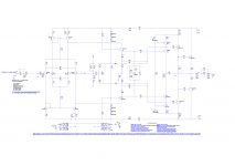
Attached are schematic and loopgain plot. Enjoy the new loops. Still sub-optimal though. 🙂
Paul
Edit: Another observation about this amp is that it can provide 500mA without switching the non conducting half off. Not sure why.
Attachments
Last edited:
Hi Guys
My comment was specifically about current sources/sinks NOT current mirrors.
Self showed that the feedback CS is faster and more accurate, but there were articles in WW decades ago illustrating the same points, so I've only ever used the feedback type since then. Cordell showed the pitfalls of the buffered references, as well, in his book.
It seems to me that cascode elements also must be considered a bit more seriously than more than just something that provides voltage compliance. A slothy cascode might have higher internal capacitances, etc, and so not improve things as much as a better device might have.
Have fun
My comment was specifically about current sources/sinks NOT current mirrors.
Yes, I understand that. I did say that I expected the CM tests to be "somewhat equivalent" and they were the best data I had until I study current sources/sinks more closely.
Self showed that the feedback CS is faster and more accurate, but there were articles in WW decades
Where did Self show this? Most of his WW articles ended up incorporated into the book and I haven't noticed it there.
A WW reference would be less convenient but still fine.
Cordell showed the pitfalls of the buffered references, as well, in his book.
He quotes lower output impedance for a buffered reference but I don't think he shows "pitfalls", can you be more specific, p. number and para.?
I suspect that it is the feedback source that has "pitfalls", in the sense that a pitfall looks OK but is actually an unpleasant surprise.
The inherent feedback loop would seem to have some risk of unexpected interaction.
This has been reported in the similar case of Baxandall current sources.
Best wishes
David
...You don't often see amps with over 100 degrees PM it has to said....
You don't often see amps that try to hit 8 MHz either😉
TPC probably requires some extra PM.
As the amp slows down (due to approach to rails or capacitive load) we lose more PM than a Miller compensated amp I think.
Hence the numbers look unfamiliar and "alien".
Have since re-done my sims for output close to the rails and now it is scary to see how much PM disappears.
Yes, didn't I say that?😉
Ric Lee has actually tested "boutique" so-called audiophile amps and most of them were intermittently unstable, presumably because the builders underestimated this.
...point is that the ULGF drops as the amplifier nears the rails.
Yes.
2uF ... certanly not worst case by my limited experience.
2uF is traditional but not very informative.
Your experience is consistent with Self and Ric Lee.
Have to run front end rails down 0.7v on OPS rails
Must say I'm not too concerned about clip behaviour that's not actually destructive.
If it clips then it's distorted by definition.
But I have JBL compression drivers so by the time they clip there are other problems - like ear injury.
Layout is critical IMHO....Understand about loop areas etc. The basics... But planes (especially)...have not been tried... planes ...scare me
Most DIY layouts waste the chance to use the two sides of a board to minimize loop area and inductance.
If there is a one sided power supply then planes can be a way to do this almost automatically.
A push pull supply (like most power amps) requires a bit more consideration.
I don't use planes but do cancel currents on opposite sides of the board.
So the effect is similar.
[Switched] rails and then questions about where to put the ...capacitors in relationship to the protection MOSFETs. And how would the MOSFETs affect the output devices?
The MOSFETs are probably superior to fuses overall.
I think the decouple capacitors should be placed downstream of the MOSFET rail switches.
They should not have sufficient capacity to destroy much.
The MOSFET resistance can be a few milliohms so no effect on the output devices at all.
Should be very superior to fuses, even the resistance is lower and more linear.
True there is much to be gained from heavier compensation.
I just meant that if you wanted to leave the front end zero capacitors off for simplicity then the compensation needed to be a bit heavier.
I have a very definite preference for simplicity, so I don't include even a capacitor without painful deliberation.
Best wishes
David
PS. I really like to line up 0dB and 180 phase lines on the plot.
Makes it much easier to interpret.
Last edited:
Hi,
your work is interesting and refreshing. Although I do not yet fully understand your compensation scheme (especially the higher-order behaviour) and although it might be counter to your basic approach of optimization, I'd like to make a proposal.
As far as I understand, the topology has the advantage that there is no really high-impedance node between inverting input and pre-driver input (or even its output). Thus, it should be possible in principle to use Miller input compensation (MIC) e.g. between pre-driver output and inverting input without wasting too much bandwidth by shunt compensation in this loop. Thus, the input stage enjoys high linearisation. (What I understood, this has been achieved.)
If you now close the global loop around the output stage, shouldn't it then be possible to use the TMC (transitional Miller compensation) trick? To my understanding, there should be no difference whether the Miller compensation spans only to the "VAS" input or to the global inverting input. Combining high ULGF in the global loop with TMC, one should get huge amounts of feedback around the output-stage (second-order characteristics).
I really appreciate your approach to try to optimize the compensation of a given architecture, that is sensible from general understanding, without resorting to established design ideas as TMC and so on. Nevertheless, isn't the above a possibility?
Kind regards,
Matthias
Hi Matthias,
Thank you for your kind words about my design 🙂 Like to try to do things differently.
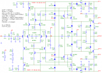
Your ideas are most welcome. I tend to end up in mental corners. I think I follow you scheme. Sounds like the original SuperTis compensation? See atached image. However, I'm struggling to use "TPMIC" as the main compensation for this amplifier. Keep ending up back at the "two pole boostrapped shunt compensation" with a little lead compensation accross the feedback resistor.
In the schematic with the "TPMIC" http://www.diyaudio.com/forums/solid-state/265449-amp-designed-during-lunch-breaks-8.html#post4186413 it appears that the MIC loop only provides extra stability due to the OPS being out of the loop at higher frequencies. Is this stability "real"? Not sure.
Still new to this loop analysis and amplifier compensation but have been wondering about this...
If you look at the LG plot above. Up to the ULGF the shunts dominate and after that my version of "TPMIC" takes over.
When driving capacitive loads or when driven close to the rails the amplifier slows down and the ULGF drops significantly. Should we be looking at the stability of the amplifier without the "TPMIC" to get an idea of the real stability at lower frequencies of ULGF? It may explain why "TPMIC" loses more PM than other forms of compensation when the amplifier is driven close to the rail voltage? At least for this amplifier...
Is it better to use "TPMIC" or use shunts to shape the NGFB loop? That way the whole amplifier is enclosed in the feedback loop. Shunt compensation is usually considered sub-optimal though?
I may well be in a mental corner with MIC... 😉
Or there may be a reason, I've yet to comprehend, why this amplifier doesn't work well with "TPMIC". 🙂
Paul
Thank you for your kind words about my design 🙂 Like to try to do things differently.
Your ideas are most welcome. I tend to end up in mental corners. I think I follow you scheme. Sounds like the original SuperTis compensation? See atached image. However, I'm struggling to use "TPMIC" as the main compensation for this amplifier. Keep ending up back at the "two pole boostrapped shunt compensation" with a little lead compensation accross the feedback resistor.
In the schematic with the "TPMIC" http://www.diyaudio.com/forums/solid-state/265449-amp-designed-during-lunch-breaks-8.html#post4186413 it appears that the MIC loop only provides extra stability due to the OPS being out of the loop at higher frequencies. Is this stability "real"? Not sure.
Still new to this loop analysis and amplifier compensation but have been wondering about this...
If you look at the LG plot above. Up to the ULGF the shunts dominate and after that my version of "TPMIC" takes over.
When driving capacitive loads or when driven close to the rails the amplifier slows down and the ULGF drops significantly. Should we be looking at the stability of the amplifier without the "TPMIC" to get an idea of the real stability at lower frequencies of ULGF? It may explain why "TPMIC" loses more PM than other forms of compensation when the amplifier is driven close to the rail voltage? At least for this amplifier...
Is it better to use "TPMIC" or use shunts to shape the NGFB loop? That way the whole amplifier is enclosed in the feedback loop. Shunt compensation is usually considered sub-optimal though?
I may well be in a mental corner with MIC... 😉
Or there may be a reason, I've yet to comprehend, why this amplifier doesn't work well with "TPMIC". 🙂
Paul
Attachments
You don't often see amps that try to hit 8 MHz either😉
TPC probably requires some extra PM.
As the amp slows down (due to approach to rails or capacitive load) we lose more PM than a Miller compensated amp I think.
Hence the numbers look unfamiliar and "alien".
8MHz... Got to have a challenge. Unfortunately, a standard blameless style amplifier just doesn't do it for me. 😉
Beginning to question whether the stability gained by TPMIC in this design is real. See my reply to Matthias.
Yes, didn't I say that?😉
Ric Lee has actually tested "boutique" so-called audiophile amps and most of them were intermittently unstable, presumably because the builders underestimated this.
Yes, but untill I re-ran the test didn't see the same loses. 😉
Ric Lee and his "Golden Pinnae" amps. I think he also suggested that the high end audiophille sound was actually caused by the instabilities.
Must say I'm not too concerned about clip behaviour that's not actually destructive.
If it clips then it's distorted by definition.
But I have JBL compression drivers so by the time they clip there are other problems - like ear injury.
This made me smile. 😉 Ear Injury...
My speakers are not that efficient (Around 93dB). So clipping may well be an issue. Although, having neighbours seems to put a limit on things. 😉
Most DIY layouts waste the chance to use the two sides of a board to minimize loop area and inductance.
Maybe because PCB layout is a very complex subject and laying out a PCB for performance doesn't always yeild the most aesthetic end result. Personally, I see it as another chance to optimise things.
I think the decouple capacitors should be placed downstream of the MOSFET rail switches.
...
Should be very superior to fuses, even the resistance is lower and more linear.
Sold. 😉
Fuses can be too slow to protect anything anyway. Experience again. 😉
Relays can't be trusted in fault conditions either.
I have a very definite preference for simplicity, so I don't include even a capacitor without painful deliberation.
Best wishes
David
PS. I really like to line up 0dB and 180 phase lines on the plot.
Makes it much easier to interpret.
There's something to be said about simplicity. Learnt from experience on this one. Why does experience have to be expensive?
I'm struggling to get an output from LTSpice that clearly shows the LG plots. The 0dB and 180 phase lines are lined up but they are not clearly visible in the attachments. It does, however, show the values for the cursors underneath the plot which may or may not be usefull.
Want to make things easy to read. So once again I'm open to suggestions to improve things.
On another topic. Been reading up about thermaltrak transistors after you mentioned them earlier in this thread. Found various solutions, including Bob Cordell's implementation. With my amp having a very low Vbe spread at the VAS could thermaltracks even be used? There must be a simple effective way of using them. 😉
Paul
Last edited:
- Status
- Not open for further replies.
- Home
- Amplifiers
- Solid State
- Amp designed during lunch breaks