Measure the DCV across the speaker terminals of each channel. Do you read more than a tiny fraction of a volt on either channel?
If so, which channel?
The thread says 3553 but the spike you posted says 3554. Which is it?
Have you done ANY work on the amp other than repairing a solder connection?
If so, which channel?
The thread says 3553 but the spike you posted says 3554. Which is it?
Have you done ANY work on the amp other than repairing a solder connection?

I ve done : pretty much all of the caps, in the regulator :2 Zener , two ttc-tta pair, 5 ic with adapters njm4580 to opa2134. It is 3553.
Does your solder have a flux core?
Do you have any additional flux?
Did you check the voltage on the regulator components to see if they were producing the correct output?
Did it ever work perfectly after replacing all of those parts?
Do you have any additional flux?
Did you check the voltage on the regulator components to see if they were producing the correct output?
Did it ever work perfectly after replacing all of those parts?
I have flux and solder , solder without flux in it.It worked just fine 3 days, I was tuning and tweeters were on mute, without moving the car.i din’t test the regulator.
I'd suggest desoldering all of those regulator connections, removing all solder and then resoldering. As they are, they don't look reliable. Then confirm that the output voltage of both regulators is ±15v.
What I don’t know is if the second row where the copper is exposed have to have continuity , because like that it have.
I don't understand. Bare copper is not a problem.
Continuity is a generally useless term. Please be specific.
Continuity is a generally useless term. Please be specific.
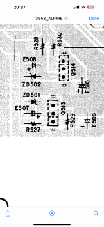
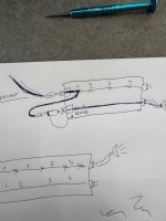
So in the picture it is a cap , a resistor and Zener , all of the right side of parts, near the transistor are touching each other
I still don't understand. Are you referring to the bodies of the components on the component side of the board?
Then I can put more solder, and solder them good, I tried to don’t touch each other as much as I could, also when the amplifier starts it stays red 1 2 seconds then it goes green , as far as protection goes. I don’t know what it should protect.
And I tested like this: rca signal on the bad channel , speaker output on good channel and the rca probe on the good channel.
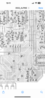
So on cb connector on the motherboard I had just louder sound, not related to music , and on ic101 on exit it mutes all the sound if I remember right.
So on cb connector on the motherboard I had just louder sound, not related to music , and on ic101 on exit it mutes all the sound if I remember right.
Attachments
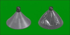
The solder that's there is garbage. It needs to be removed 100% and the connections resoldered. The connections should be uniform/symmetrical and have a profile somewhere between the shape of the two in the graphic below.
I don't understand post #35 or 36. You're going to have to be far more specific in the questions.
I don't understand post #35 or 36. You're going to have to be far more specific in the questions.
Attachments
on 35: I tried to test the bad channel to see where the signal stops , touching the board in different points, if I had sound I know that the signal is ok till that point.let’s say other way : touching in different points will close the circuit thru a good channel.
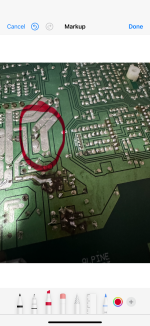
And 36: on the picture there are 3 big marks separate of each other , how could I know if they have to touch each other(common) trace or separate.
And 36: on the picture there are 3 big marks separate of each other , how could I know if they have to touch each other(common) trace or separate.
What are you using to test for signal?
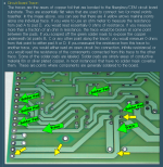
The darker areas are the bare board (fiberglass). The lighter areas are tinned copper circuit board with a green transparent solder mask. The gray areas inside the lighter areas are areas where the solder mask was not applied. You're seeing the solder that's tinning the board.
The darker areas are the bare board (fiberglass). The lighter areas are tinned copper circuit board with a green transparent solder mask. The gray areas inside the lighter areas are areas where the solder mask was not applied. You're seeing the solder that's tinning the board.
- Home
- General Interest
- Car Audio
- Alpine 3553