Yeah I know I am almost to the point of putting Alpha 20 back in and calling
Nirvana a no go for me!
Scott
Nirvana a no go for me!
Scott
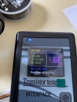
Looking at the voltages in post 2506, it seems both transistors have 4-5volts between gate and source, but the sources are 19-20V instead of +/- 0.4V (also assume the Pchannel drain is -25V not +25V). Maybe the outputs are OK but there is an issue with the LTP or feedback causing the DC offset.
I replaced the N mosfet reinstalled and same issue the gate has 0v the drain and source have 25v I have no idea!
Could v111 and v112 be causing the N channel not to kick on?
Only other thought is maybe trying a new diode on the snubber board just a thought?
Scott
Only other thought is maybe trying a new diode on the snubber board just a thought?
Scott
https://www.mouser.com/datasheet/2/308/1/KSC3503_D-2314728.pdf
Check the orientation of your V115 transistor please. Looks reversed.
Best,
Anand
Last edited:

Anand,
Great catch on the V115 they are reversed!
Thank you so much.
I will get those flipped around and give feedback Tomorrow if I get her going.
Scott
Great catch on the V115 they are reversed!
Thank you so much.
I will get those flipped around and give feedback Tomorrow if I get her going.
Scott
Wow, good catch. I almost did the same thing, but caught it before I cut the leads. Easy mistake to make.
Fingers crossed that works for ya!
Reading debugging threads always helps me learn something. Referencing to X’s post #2503…and reading the 1st page of this thread specifically noting Hugh’s original schematics (where voltages are printed)…

Study the voltages above carefully. Particularly the G,D,S voltages of the MOSFETS.

In the annotated schematic above, which is best schematic to use when building the current version of the Alpha Nirvana boards, It appears that V115 is involved in turning “on” the N channel MOSFET via the positive voltage rail (along with voltage dropping resistors R121,R122 and cap).
Similarly, V131 is involved in turning “on” the P channel MOSFET via the negative voltage rail (also with voltage dropping resistors R131,R132 and cap).
If either V115 or V131 are not installed properly (wrong gender or flipped around) then the circuit isn’t complete and can’t work.
V121, V122 and H121 are really there for the cool red LED clipping light. They were never there in Hugh’s original schematic, so I don’t see them in a primary role. The light will start to come on when the gate voltages increase (as they do when the amp puts out higher and higher output power due to increasing input voltages). It’s a really cool trick that Hugh threw in there 👍.
Anyway…
I hope you are listening to some fine tunes tomorrow 😉.
Then you can let us know if a 5U/300 can handle the dissipation 🥵!!!
Best,
Anand.
Reading debugging threads always helps me learn something. Referencing to X’s post #2503…and reading the 1st page of this thread specifically noting Hugh’s original schematics (where voltages are printed)…
Study the voltages above carefully. Particularly the G,D,S voltages of the MOSFETS.
In the annotated schematic above, which is best schematic to use when building the current version of the Alpha Nirvana boards, It appears that V115 is involved in turning “on” the N channel MOSFET via the positive voltage rail (along with voltage dropping resistors R121,R122 and cap).
Similarly, V131 is involved in turning “on” the P channel MOSFET via the negative voltage rail (also with voltage dropping resistors R131,R132 and cap).
If either V115 or V131 are not installed properly (wrong gender or flipped around) then the circuit isn’t complete and can’t work.
V121, V122 and H121 are really there for the cool red LED clipping light. They were never there in Hugh’s original schematic, so I don’t see them in a primary role. The light will start to come on when the gate voltages increase (as they do when the amp puts out higher and higher output power due to increasing input voltages). It’s a really cool trick that Hugh threw in there 👍.
Anyway…
I hope you are listening to some fine tunes tomorrow 😉.
Then you can let us know if a 5U/300 can handle the dissipation 🥵!!!
Best,
Anand.
Thank you Anand!
A fine diagnostician!
I was a bit slow off the mark here; my mind is a bit cloudy at present but generally I'd suggested to Scott he check all the polarised components, particularly the zener on the clipping indicator and the KSC3503. Absolutely a common issue putting in TO92 and TO126 transistors in place the wrong way around.
Hugh
Thanks Hugh, your tutelage is always appreciated. And I am stoked that the voltages were printed on the original schematic. It helps to trace things out and understand the circuit for us neophytes!
All this blah, blah, blah is useless, wait till Scott hears it! Fingers crossed !!
!!
Best,
Anand.
All this blah, blah, blah is useless, wait till Scott hears it! Fingers crossed
!!Best,
Anand.
Hugh,
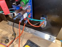
Well I was taking off those molex connectors to wire the snubber boards Directly to the board and I pulled one of the contacts up,me being a knucklehead!
Anyway X is sending me a new board
I will get it together and going quickly I hope.
Scott
Well I was taking off those molex connectors to wire the snubber boards Directly to the board and I pulled one of the contacts up,me being a knucklehead!
Anyway X is sending me a new board
I will get it together and going quickly I hope.
Scott
Oy vey. That sucks man! Was it the snubber board that got affected or the main Alpha Nirvana board 😱 ???
Best,
Anand.
Best,
Anand.
- Home
- Amplifiers
- Solid State
- Alpha Nirvana 39w 8ohm Class A Amp