Guys, I would like to build this amp, have the components. Can I ask where or who might have pcb's or gerber files available and what schematic was used for the particular pcb. I see many different circuits throughout this thread, many thanks.
The last build done here by lganymis apparently use Alex s PCB wich lack a late update that can be easily
implemented in the board since that s just a 220pF cap that can be soldered in parralel with the relevant resistance,
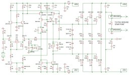
Here the updated schematic that include this cap with the reference C14 as well as the PSU with dual rails
for the driver and output stage, a single pair of rails can be used but then the driver supply voltage will sag
along with the OS supply voltage, the dual rails allow the driver to benefit from the peak voltage of the PSU
permanently wich increase the output power capability.
implemented in the board since that s just a 220pF cap that can be soldered in parralel with the relevant resistance,
Here the updated schematic that include this cap with the reference C14 as well as the PSU with dual rails
for the driver and output stage, a single pair of rails can be used but then the driver supply voltage will sag
along with the OS supply voltage, the dual rails allow the driver to benefit from the peak voltage of the PSU
permanently wich increase the output power capability.
Attachments

Thanks for the reply, I wonder if Alex has boards or can make the gerber files available? I might have to PM him.
@Iganimys - where did you get the pcb's for your build - nice work by the way.
@Iganimys - where did you get the pcb's for your build - nice work by the way.
I've been lurking here also Gary, hehe.
Post#319 : Alex shared the gerbers for board version Rev4.5 (Iganimys build)
But later in post#378 Alex posted an image of layout Rev4.6 that might have the correction wahab mentioned. But couldn't find any gerbers for that one.
Post#319 : Alex shared the gerbers for board version Rev4.5 (Iganimys build)
But later in post#378 Alex posted an image of layout Rev4.6 that might have the correction wahab mentioned. But couldn't find any gerbers for that one.
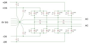
We have the PCB design for the circuit in post #1, i.e. the titled circuit.

We also have both the original devices, as well as proposed substitutes.
But as usual, we shall not publish until it is built, fully tested, and auditioned.
We shall be using double -die Exicon lateral MOSFETs for the output stage.
Simply because we have them for other projects (incl. The F5XL).
BTW, only interested in the original topology using JFETs and lateral MOSFETs.
www.diyaudio.com/community/threads/all-hitachi-lateral-fet-amplifier-for-diy-described-by-paul-kemble.220923/post-7805123
Patrick
Last edited:
We meet again Vunce, I looked through the thread and could not find any gerbers - will have a look at that post again. I saw the Rev 4.6 layout.
Was interested in the Rev 5 layout Alex posted in post #358 using TO3 outputs as I have J50/K135 Hitachi's.
I will PM Alex to see if I can get an answer - after all those posts were 12 years ago now.
Will keep an eye out Patrick for your design of the original circuit - which is really what I was interested in.
Hopefully you will get a reply from Alex regarding 4.6 and 5.
Rev5 would have a cool nostalgia feel to it.
Nice Patrick!
Rev5 would have a cool nostalgia feel to it.
Nice Patrick!
Of course you don't need to wait for us.
The thread owner already posted a PCB design.
www.diyaudio.com/community/threads/all-hitachi-lateral-fet-amplifier-for-diy-described-by-paul-kemble.220923/post-3197833
Ours looks different :

Remember of course that this is Class AB with 200 mA bias at the output stage.
Patrick
The thread owner already posted a PCB design.
www.diyaudio.com/community/threads/all-hitachi-lateral-fet-amplifier-for-diy-described-by-paul-kemble.220923/post-3197833
Ours looks different :
Remember of course that this is Class AB with 200 mA bias at the output stage.
Patrick
Last edited:
Revision of the amp was made long ago but unfortunately after the PCBs were designed, so none include this cap,
wich is not that important since it can be soldered below the PCB at the resistance ends.
I didnt post it because the amp went out of scope quite a long time until i realised that a user
did a build in 2023 and eventualy got a slight issue when using different transistors, wich prompted me to point
what is perhaps the cause of his issue, hope that he ll see the mod although he said that it worked well ultimately.
Thanks for the reply, I agree the cap C14 can easily be added across R4. Did you build the amp as per your post #462 and was happy the way it performed and tested?
Actually i didnt build this amp, i engaged in this design after i simulated the one on post 1 and found that it was trash to say the least, and much inferior to the ubiquitous and basic schematic that originate from their most known application note.
Some people who have not forcibly deep pockets would waste laterals fets, and money, in a dud that is well below the compact discs THD wise and barely HiFi even in respect of the DIN 45500 standard when accounting its catastrophic 46 dB PSRR, indeed Hitachi themselves never used fets for the VAS part of their commercial amplifiers and that s for a reason.
For listening tests lganymis as well as another user gave their impressions, wich are very favourable since there s nothing
that is improvised or revolutionary, it s just following Hitachi s design guidelines for their laterals fets powered amps.
What caught my attention of the circuit in post #1 was the quote in the original webpage :
https://www.angelfire.com/sd/paulkemble/sound7g.html
Alister notes that
"For whatever reason, the thing worked very well. I was doing an MSc in the Audio engineering lab under Malcolm Hawksford at Essex University at the time. We knocked some up and were quite taken aback by how good they were - especially as we were in a 'mode' with our designs to see just how complex we could make them. The Hitachi Mosfet datasheet (and thinking back, it must have been early '80s) generated a host of copies. The Maplin Mosfet amp kit was well known. The current BK Electronics modules look as though they're based on it and there were innumerable commercial clones. It's one of those very simple circuits (like JLH's 10W class A) that somehow just seem to get it right. Particularly, as we found in Hawksford's lab, if you use two of them as a "Balanced" amp - a finding which set some of us off on a search for the "Earth effect" on the assumption that the improvement was largely down to balanced connection keeping high currents out of the earth connections. Malcolm actually published a number of AES papers (the "Pontoon" amplifiers) triggered by our investigations of these Balanced Mosfet amps."

So apparently, someone from the Hawksford research group did build and was notably impressed.
But the only way to find out is to build and listen, exactly what we plan to do.
😊
Cheers,
Patrick
https://www.angelfire.com/sd/paulkemble/sound7g.html
Alister notes that
"For whatever reason, the thing worked very well. I was doing an MSc in the Audio engineering lab under Malcolm Hawksford at Essex University at the time. We knocked some up and were quite taken aback by how good they were - especially as we were in a 'mode' with our designs to see just how complex we could make them. The Hitachi Mosfet datasheet (and thinking back, it must have been early '80s) generated a host of copies. The Maplin Mosfet amp kit was well known. The current BK Electronics modules look as though they're based on it and there were innumerable commercial clones. It's one of those very simple circuits (like JLH's 10W class A) that somehow just seem to get it right. Particularly, as we found in Hawksford's lab, if you use two of them as a "Balanced" amp - a finding which set some of us off on a search for the "Earth effect" on the assumption that the improvement was largely down to balanced connection keeping high currents out of the earth connections. Malcolm actually published a number of AES papers (the "Pontoon" amplifiers) triggered by our investigations of these Balanced Mosfet amps."
So apparently, someone from the Hawksford research group did build and was notably impressed.
But the only way to find out is to build and listen, exactly what we plan to do.
😊
Cheers,
Patrick
Yes from the article it looks like he was referring to the BJT/fet design and not the all fet design as shown in post #1
Patrick, time will tell we look forward to what your design turns out like - if all is well, I assume you will be doing a GB for at least pcb's and maybe active's based on your final testing/listening.
Patrick, time will tell we look forward to what your design turns out like - if all is well, I assume you will be doing a GB for at least pcb's and maybe active's based on your final testing/listening.
From another read of this thread, it looks like only two members have built the amp on the pcb design done by Alex with the schematic as shown in post #462 by wahab. Maybe there are more but have not posted in the thread.
What caught my attention of the circuit in post #1 was the quote in the original webpage :
https://www.angelfire.com/sd/paulkemble/sound7g.html
The guy is talking of the bipolar driver version not of the amp in post 1.
Beside he reproduced the text from Hitachi application note word by word without even giving any credit to the original authors,
i have the full AN, the graphs are also extracted from this AN, so you re using the numbers of an amp and are attibuting them
to another one.
Anyway i have no PCB or componenets to sell and no vested interests contrary to some people who are promoting whatever
can be used as $ printing press, if i did read it right you are on the occasion doing some business by here, so i can understand that you re promoting whatever can eventualy yield some profits no matter the real technical qualities of the designs.
Attachments
Last edited:
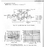
This is how I read the Paul Kemble webpage :
"A second more complex version using FETs throughout was also described. This was a DC design with low-impedance offsetting applied to the input pair, with stabilisation of their feeds and a separate supply for the input and driver stages."
followed by the schematics with all FET, then by the THD plot as shown in post #474 above, then :
"Alister note that, for whatever reason ....."
I don't think I can conclude he was referring to the BJT version.
This plot below is from the one with BJT VAS and only lateral MOSFET OPS.
Everyone can draw his own conclusions.

In any case, I prefer all FET designs, my personal taste.
Patrick
"A second more complex version using FETs throughout was also described. This was a DC design with low-impedance offsetting applied to the input pair, with stabilisation of their feeds and a separate supply for the input and driver stages."
followed by the schematics with all FET, then by the THD plot as shown in post #474 above, then :
"Alister note that, for whatever reason ....."
I don't think I can conclude he was referring to the BJT version.
This plot below is from the one with BJT VAS and only lateral MOSFET OPS.
Everyone can draw his own conclusions.
In any case, I prefer all FET designs, my personal taste.
Patrick
Simulators allow how us to check the perfs and relevancies of designs before engaging or advising people to build them,
if you prefer what is nice looking to your eyes so good, personaly i wouldnt buy on something just on the appearances
and psychological perception, i let this to people who believe the words of dreams merchants or are those merchants themselves,
so in a few words myself i prefer what pass the simulators tests, rest is fairy tales from people who are accustomed to convince
the unsuspecting crowd.
Do sims and post numbers, i m not interested in an hollow debate, so far i m the only one who did so with the amp
in post 1 and it s obvious that it s vastly inferior to the simplistic Hitachi bipolar driver, let alone to the iteration
i did in this thread.
Did that months ago.
www.diyaudio.com/community/threads/all-hitachi-lateral-fet-amplifier-for-diy-described-by-paul-kemble.220923/post-7805123
But I rather believe in real builds and measurements, as shown above for both versions by Alister Sibbald.
Cheers,
Patrick
www.diyaudio.com/community/threads/all-hitachi-lateral-fet-amplifier-for-diy-described-by-paul-kemble.220923/post-7805123
But I rather believe in real builds and measurements, as shown above for both versions by Alister Sibbald.
Cheers,
Patrick
- Home
- Amplifiers
- Solid State
- All Hitachi Lateral FET amplifier for DIY described by Paul Kemble