It was measured (long time ago) with a scope with a SW TFT function. Did not found the screenshots back. I have changed to another pcb layout after this measurement. Hopefully soon a can do another measurement. But the slope upwards is strange. The gain is increasing in the lower freq? Never saw this as far I can remember. Did you do do a 20-20K sweep?
My advice was just for test.Thanks for the suggestion, Dmitriy.
But what is the logic behind that? Why LSJ74's are not good where they were planned to be good and why 2SJ103 is better and should work? I'd love to learn in the processes and understand the reasoning.
Also, 2SJ103 is out of production, as I understand, so getting them from eBay involves some risk of counterfeit, I suppose.
J103 was the easiest jfet to find in local shop for me.
Try to replace j74's with another pair of any similar jfets. You'll get another sound quality, but you'll understand, if j74's were guilty.
It was measured (long time ago) with a scope with a SW TFT function. Did not found the screenshots back. I have changed to another pcb layout after this measurement. Hopefully soon a can do another measurement. But the slope upwards is strange. The gain is increasing in the lower freq? Never saw this as far I can remember. Did you do do a 20-20K sweep?
Well, the first day I built it (with the store supplied mosfets and bad thermopads) my measurements showed
THD 0.06% right and 0.09% left channel at 1W/8ohm, and
THD 0.27% right and 0.39% left channel at 10W/8ohm.
But that is long gone, now I have THD 0.39-0.56% at 1W and even above 1% at some time 🙁
But what makes me crazy is the LTSpice simulation!
My simulation shows me THD 0.22% at 1W/8ohm!!!
Harmonic Frequency Fourier Normalized Phase Normalized
Number [Hz] Component Component [degree] Phase [deg]
1 1.000e+3 4.077e+0 1.000e+0 -0.31∞ 0.00∞
2 2.000e+3 3.738e-4 9.168e-5 -26.47∞ -26.16∞
3 3.000e+3 1.174e-4 2.879e-5 26.70∞ 27.01∞
4 4.000e+3 2.318e-5 5.685e-6 -173.79∞ -173.48∞
5 5.000e+3 1.641e-5 4.025e-6 177.72∞ 178.03∞
6 6.000e+3 1.326e-5 3.252e-6 174.73∞ 175.04∞
7 7.000e+3 1.140e-5 2.796e-6 173.93∞ 174.24∞
8 8.000e+3 9.978e-6 2.447e-6 173.09∞ 173.40∞
9 9.000e+3 8.871e-6 2.176e-6 172.21∞ 172.52∞
10 1.000e+4 7.988e-6 1.959e-6 171.34∞ 171.65∞
Total Harmonic Distortion: 0.009652%(0.221822%)
So what can I expect from the actual build then? 😕
And the same LTSpice simulation of F5 shows THD 0.005% with my actual build measuring at THD 0.01% - so I'm inclined to believe that simulations are quite ok.
But then, my build behaves as expected! And I'm totaly confused! 😱
Does anyone see any mistatakes in component values or something on the simutation?
I mean, I would like to have at least the simulation giving me the ecpected THD of about 0.06%...
My advice was just for test.
J103 was the easiest jfet to find in local shop for me.
Try to replace j74's with another pair of any similar jfets. You'll get another sound quality, but you'll understand, if j74's were guilty.
I did not find any other J103 but Toshiba 2SJ103, and these, unfortunately, are not easily available in any store neareby here.
simple as that - your sim is no good, check some other models
regarding real amp - if you are doubting you JFets, check them out of circuit
for amp, test purpose, you can use even BC556 in place of JFets, with rebias of LTP CCS
regarding real amp - if you are doubting you JFets, check them out of circuit
for amp, test purpose, you can use even BC556 in place of JFets, with rebias of LTP CCS
Yeah, I was playing with the simulation today and found out that FFT becomes fine if I eliminate C1 or change it to 100uF instead of 1uF. I was also suspecting that my simulated measurements without any initial time before the circuit settles down could be wrong. And this is the case, I think. And then I tried to introduce a 1 sec initial delay into the simulation. The FFT I got is totaly different and THD is just 0.01% (attached for the reference). Well, this was good new experience for me too 🙂
Now, simulation clarified and out of the way, back to the real thing.
Thank you, Zen, for suggesting BC556 as a temporary replacement.
These are, of course, easily available. Should I match them somehow before I put them into the circuit for a test? And how should I rebias the CCS? Some resistors in R6 and/or R30 instead of the jumpers?
And how could I test LSJ74's out of circuit? Universal transistor checking tool could be of any help here?
Attachments

And how could I test LSJ74's out of circuit? Universal transistor checking tool could be of any help here?
Something like this: https://www.amazon.com/Pocketable-M...t=&hvlocphy=9010231&hvtargid=pla-845729973092
Not for matching transistors, just to check and see they are working.
Best,
Anand.
Yea, thanks, I have ordered one of these a few weeks ago from China already.
But could they be useful in my case? Can it be that the tester shows them being ok, but they would still be noisy or giving too much distortion?
But could they be useful in my case? Can it be that the tester shows them being ok, but they would still be noisy or giving too much distortion?
its basically a go no go tester. Jfets may show source drain leads reversed. At least it did with my LSJ74's. Its great for checking parts before stuffing a board
Yeah, I was playing with the simulation today and found out that FFT becomes fine if I eliminate C1 or change it to 100uF instead of 1uF. I was also suspecting that my simulated measurements without any initial time before the circuit settles down could be wrong. And this is the case, I think. And then I tried to introduce a 1 sec initial delay into the simulation. The FFT I got is totaly different and THD is just 0.01% (attached for the reference). Well, this was good new experience for me too 🙂
Now, simulation clarified and out of the way, back to the real thing.
Thank you, Zen, for suggesting BC556 as a temporary replacement.
These are, of course, easily available. Should I match them somehow before I put them into the circuit for a test? And how should I rebias the CCS? Some resistors in R6 and/or R30 instead of the jumpers?
And how could I test LSJ74's out of circuit? Universal transistor checking tool could be of any help here?
nope, 1uF - value - can't be a problem
find real problem in your sim
BC- matched with Hfe on your DMM or with universal thingie, good enough
for these - decrease LTP current (0 output DC offset is what you observe and what is your goal)
sole programming resistor is what you need to change (up in value - put trimpot if you didn't already)
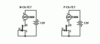
check JFets in simple matching jig, small 12V PSU or 9V battery
Attachments
What is the recommended size of the heat sink, if they are mounted outside the case (one channel per heat sink)?
Hi again. Sorry for asking so many questions. I hope I'm going up the learning curve 🙂
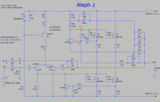
Before ripping apart my Aleph J again and desoldering JFETs I wanted to poke arround with the multimeter. And I noticed a strange (at least for me) thing arround the bias setting resistors R27 on both boards.
I noticed that if I measure DC with the reference to ground at one side of R27 (marked T1 on the attached scematics) I get 4.8V (and that also agrees with the simulation). But when I measure DC on the other side of R27 (point T2), I get negative -0.25 to -0.35 (it's changing every minute or so). And when I measure DC across R27, I get about 3.86-4.00V. These measuments do not match in my understanding. And in the simulation numbers do match (0.6V at T2 and 4.2V across R27).
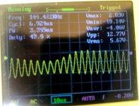
Then I measured AC with the reference to ground at poin T2 and got ~6VAC. And checking that point with the oscilograph I see the picture attached: some 12Vpp at a frequancy of about 140-150 KHz!
Does it says something? Is it some sort of oscillation?
Please bear with me if I'm poking arround with no sense.
Sincerelly,
-Alvydas
Before ripping apart my Aleph J again and desoldering JFETs I wanted to poke arround with the multimeter. And I noticed a strange (at least for me) thing arround the bias setting resistors R27 on both boards.
I noticed that if I measure DC with the reference to ground at one side of R27 (marked T1 on the attached scematics) I get 4.8V (and that also agrees with the simulation). But when I measure DC on the other side of R27 (point T2), I get negative -0.25 to -0.35 (it's changing every minute or so). And when I measure DC across R27, I get about 3.86-4.00V. These measuments do not match in my understanding. And in the simulation numbers do match (0.6V at T2 and 4.2V across R27).
Then I measured AC with the reference to ground at poin T2 and got ~6VAC. And checking that point with the oscilograph I see the picture attached: some 12Vpp at a frequancy of about 140-150 KHz!
Does it says something? Is it some sort of oscillation?
Please bear with me if I'm poking arround with no sense.
Sincerelly,
-Alvydas
Attachments
It could be that the probes are causing oscillations.
In fact, this is how I used to find the bad MOSFET, out of many (let's say 12 MOSFETs, or more), without desoldering them. I used to place the probe on the gate stopper resistors, one at a time. The faulty one (faulty MOSFET) would cause oscillations (start to oscillate), with the probe connected to its gate stopper resistor.
You may have faulty MOSFET(s). I am not sure if you have replaced them or not...
I'm thinking here out loud... you should probably get a new set of PCB's and start fresh, with new transistors. Just make sure that you use the antistatic wrist strap properly grounded, at all times (especially when matching the JFETs), but also, later during the assembly. This includes the MOSFET's as well.
Once they are soldered, they are safe.
Last edited:
Thanks, Boky.
My full story goes like this.
I built Aleph J in mid February, powered it up and started doing some measurements. At that time I noticed that mosfets run a bit hotter than expected (it was about 60-70C at the case) and this was the first time that I used new type of thermal interface in my build. Anyway, I continued with my measurements and had THD of 0.06% and 0.09% at 1W on left and right channels. So that was about fine.
But then I noticed that mosfets on my left channel became too hot, on one of them I measured was close to 150C at the drain pin! So I turned it off, consulted the forum and found out that my thermal interface is crap, so I ordered aluminum oxide pads and replaced them.
With the aluminum oxide pads, mosfets ran at about 50C, bias was ok, DC on output was fine, but THD measurements showed that at 1W I had 0.46% THD on the left channel and normal 0.06% on the right channel. Again, wise people on the forum suggested that I could have scorched the mosfets, so I ordered a tube of them from Mouser, did the matching myself, found a lot of very well mathed mosfets and exchanged all of them on both channels (left channel was suspected, right channel had to be ok as it was never so hot as the left).
With the new mosfets, I powered on the amp and started with the hum/buzz detection with the headphones connected to the outputs. What I found was that the right channel was almost ideally quiet, very low buzz, but the left channel was noisy. Then I hooked up the Focusrite for THD measuments and found out the same bad THD on the left channel (about 0.4% at 1W as before). So, new mosfets did not help. I expected to have perfect right channel (as it was so quiet), but unfortunatelly I found out that the same problems started on the right channel - THD became 0.56% at 1W and the big buzz with high pitch elements also started on that right channel. So now I have both channels very noisy and with high THD 🙁
Though bias voltages accross the power resistors are now perfect: with new well matched mosfets they all are in the range of 398-402 mV. DC on the output is also fine, but has a strange "feature" that it stays well about 0V when inputs are shorted, but jumps to -50mV when the inputs are opened. Both channels behave the same. Though at that time in the beginning, when the right channel was still good, DC offset was 0V on it independent of the open/shorted input.
So, now the best suggestion I have is to change JFETs. But I am a bit reluctant, as I want to understand what is really going on. The right channel seamed fine initially, but broke after some time. If JFETs are damaged, are there reasons for that? If I put new JFETs, can it be that they would become damaged again, because the root cause is somewhere else?
I do not have resistors on the gates of JFETs (J1 and J2 are jumpers). I also have jumpers in R6 and R30 as recommended in the buid guide. But the guide does warn about occasional oscillation that happens to some builds. My experience is very short, and I never faced oscillation before, so I know nothing about it.
But my top wish is now to be able to diagnose a real problem somehow before starting to put new parts in all the possible places. I want so much to see the reasons before I do something.
Concerning the handling of transistors, I am aware of the danger of the static discarge, though I do not have antistatic wrist strap. But I never noticed any discarge when handling them, nor I had these problems with any other of my builds.
I understand that all these stories could be boring to others, but would be grateful for all the good people here who would spend their time to guide and teach me
I don't know if it will help you and if I have already mentioned it, but when I overheated one channel of the M2x, I had to replace the Panasonic 0.47R resistors. I didn't have a pure sine wave. After replacing them, everything returned to normal
Thanks @darrr. Yes, you did tell this and I have this in mind, but this is strange to me, as these 0.47ohm resistors should be withstanding 3W and in AJ they run at about 0.34W (some 9 times less). And even if they got some heat from mosfets for some short time - could they be so sensitive to care? Also, as I measure bias voltages on them so stable now, I think they should be ok.
Can resistors really introduce so big distortion?
Especially with the fact that in the beginning everything looked fine, but then problems started? I'm not experienced enough to judge that, but it looks so weird to me.
Can resistors really introduce so big distortion?
Especially with the fact that in the beginning everything looked fine, but then problems started? I'm not experienced enough to judge that, but it looks so weird to me.
So that's not a good track, and mine had visible signs of overheating. Good luck in your search 🙂
The JFETs should not be handled without an antistatic strap properly worn and grounded. They can get damaged just enough to still measure almost perfectly but will give trouble in the circuit if mishandled.
You replaced the MOSFET's, but did you replace the 0.47ohm/3W resistors as well?
Oscillations can be easily observed on oscilloscope.
Connect the tone generator to input, and 8ohm/50W resistor to output. Start with a 200mV signal and slowly start increasing the frequency while observing the output. One probe can go to a binding post (output), the other to R11 and R12 junction. If you see oscillations, replace the JFET's. Repeat the test.
I am not sure if you posted the photos of your build. Maybe you have wiring issues...?
Have a look at the attached photo. The orientation and placement of PCB's and CL60 ensure the shortest possible wiring - all wiring!
The mains wiring is only 10cm long including the CL60; it runs underneath the transformer mounting metal plate.
DC wiring is also the shortest possible because the PS PCB lugs are now in the middle of the amp.
The 2X20V AC wiring is 25cm long (runs underneath the power supply PCB; the wires are fed from underneath the PCB and then soldered from the top)
People report oscillatons.... but usually, there's a plethora of other PCB's (various protections, unnecessary terminal blocks, signal wiring running in parallel to mains wiring, input wiring running in parallel to speakers wiring) used in those cases - wire spaghetti everywhere.... any amp will suffer an increase in THD and noise, and may even oscillate if you do this to it. But, this goes unnoticed because not many decide to check their builds.
Those who do tend to check their builds, have already built it properly 🙂 in the first place.
Attachments

- Home
- Amplifiers
- Pass Labs
- Aleph J illustrated build guide